The 12th (2012) Yamazaki-Teiichi Prize Winner Measurement Science and Technology
Development and standardization of semiconductor characterization technique using photoluminescence
| Winner | ||
|---|---|---|
| Michio Tajima | ||
| History | ||
| Mar. 1975 | Completed Doctor’s Course, Graduate School of Engineering, the University of Tokyo | |
| Jul. 1975 | Joined the Electrotechnical Laboratory, the Ministry of International Trade and Industry | |
| Mar. 1989 | Associate Professor at the Institute of Space and Astronautical Science, the Ministry of Education | |
| Oct. 1992 | Professor at the Institute of Space and Astronautical Science, the Ministry of Education | |
| Apr. 2000 | Director at the Institute of Space and Astronautical Science / Japan Aerospace Exploration Agency | |
| Mar. 2011 | Retired from the Institute of Space and Astronautical Science / Japan Aerospace Exploration Agency Emeritus Professor at the said Institute | |
| Jul. 2012 | Processor at Organization for the Strategic Coordination of Research and Intellectual Properties, Meiji University | |
| Present | ||
Reason for award
Dr. Michio Tajima found in 1978 that the intensity ratio of light emission caused by impurities in Si crystals to light emission inherent to Si increases nearly proportionately to the impurity concentration by means of a photoluminescence technique that employs laser light as an excitation source. This technique was an epoch-making one that provides both sensitivity and spatial resolution that have achieved more than a double-digit increase as compared with those obtained by the infrared absorption spectroscopy that had been generally used theretofore. In particular, the sensitivity of detection shown was a marvelous value of 80 ppq (8 x 10-14) in atomic ratio.
He further devised and implemented a world-scale round robin test (joint work that evaluates the same specimens by circulating them among multiple testing institutions) with a view to standardizing this technique, and not only realized the establishment of a domestic standard (JEIDA-45 Standard), but the ASTM F1389-92 Standard, i.e. the "Standard Test Methods for Photoluminescence Analysis of Single Crystal Silicon for III - V Impurities," that have worldwide authority (1992). Luckily, thanks to efforts made by Dr. Tajima as well as those concerned, this evaluation method was incorporated in 1996 into JIS H 0615 in Japan and further into the international standard SEMI MF 1389-0704, thus having been widely utilized since then as an evaluation standard in the manufacture of semiconductors.
Also, use of this technique has been enlarged, in addition to the evaluation of Si, to the defect analysis in GaAs and further SiC, etc. as well, which are drawing attention for power device applications.
In retrospect, Japan has been forced to take part in tough fights in many industrial fields by the strategies for international standardization mainly employed by EU and patent strategies of the United States. The semiconductor industry is not an exception, either. It is no exaggeration to say that among them, strategies for the obtainment of relevant patents and further for international standardization that were deployed by Dr. Tajima are precisely the indexes of cutting-edge measurement and evaluation technologies.
Due to the aforesaid reasons, Dr. Michio Tajima will be an awardee of the 12th Yamazaki-Teiichi Prize in the field of measurement and evaluation.
Background of research and development
The major raw materials that support today's electronic industry are the single-crystalline silicon (Si), and its manufacture requires ultra-high purity raw materials of which residual impurities are less than 100 ppt (one ten-billionth) in atomic ratio. As a technique for evaluating such an ultra-minute amount of impurities, the infrared absorption spectroscopy was conventionally employed, but its performance was such that measurement could only be made by increasing the thickness of the specimens to be measured to around 10 mm. Whereas, the awardee has demonstrated that by using specimens of which thickness is only several hundred μm, impurities of 0.1 ppt (one 10-trillionth) can be detected and its concentration can be determined by means of a photoluminescence (PL) technique using laser light as an excitation source.
Furthermore, the awardee has shown that this technique is effective for the evaluation of crystalline defects as well, and in order to evaluate the defects in GaAs wafers for high-speed devices, ultra-thin SOI wafers that attract attention as a substrate for the next generation LSIs, and SiC wafers on which great interest is shown as low-loss power devices, he created various types of equipment that are full of originality one after another. In recent years, he has invented a new technique toward the evaluation of defects in multicrystalline Si wafers for solar cells, an this technique attracts attention as an epoch-making technology.
Achievements
The awardee achieved success in the measurement of PL from Si with good reproducibility, by disproving the common sense at the time that "Si is an indirect gap semiconductor, and since its light emission becomes very small, and so it cannot be used for the evaluation" and through the devising of a plan for the specimen position adjustment method by making use of multiple laser beams, and others. Figure 1 shows a PL spectrum from an ultra-high impurity Si crystal, in which boron (B) and phosphorus (P) that are the impurities on the order of ppt (one trillionth) are clearly observed. And an impurity quantification technique has been invented which is based on discovery that the intensity ratio of light emission caused by impurities in relation to the light emission inherent to Si is nearly proportionate to the impurity concentration. This relationship for B and P impurities is shown in Fig. 2, and is used as a calibration curve for the impurity quantification. The awardee achieved standardization by planning and implementing the world-scale round-robin measurement, and moreover by making standard samples for each of the impurities, and by distributing them among the major institutions in the world. This technique has been registered officially in the American Society for Testing and Materials (ASTM) for the first time as Japan's own technology, and thereafter has also been adopted as a JIS standard (JIS H 0615) and SEMI standard (MF1389-0704) as well.
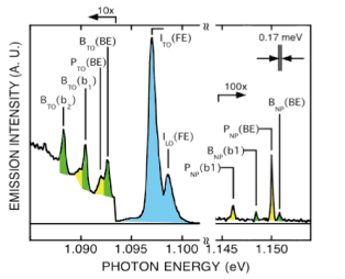
Fig. 1 PL spectrum of high purity Si crystal
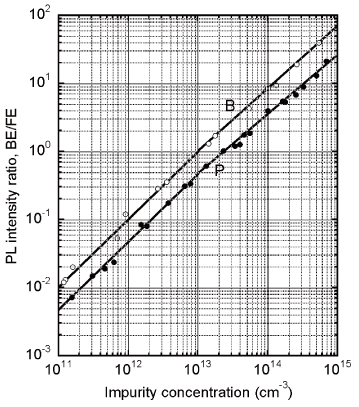
Fig. 2 Calibration curves of PL method for impurity quantification in Si
Subsequently, attention was focused on deep-level PL as caused by defects that had remained as an unexplored field in the semiconductor physics, and the origin of the defects has been elucidated through its analysis, and at the same time it has been demonstrated that semi-quantitative analysis can be carried out. By the development of the measuring method for PL excitation spectroscopy in the infrared region, room temperature PL wafer mapping method, and ultraviolet-laser-excited condensate luminescence method, high-precision and high-speed evaluation of defects in semi-insulating GaAs wafers and ultra-thin silicon-on-insulator (SOI) wafers has been realized. These techniques have been deployed in the evaluation of wide--gap semiconductor SiC wafers as well, and it has been clarified that structural defects such as dislocation and stacking fault, etc. can be detected nondestructively and under the conditions of high speed and high resolution. Figure 3 shows the distribution of defects in SiC wafers by means of PL mapping, in which micropipes and dislocations are clearly detected.
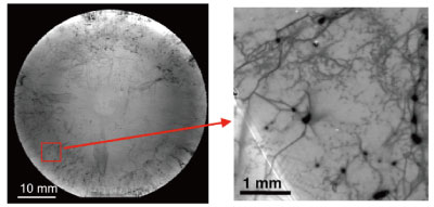
Fig. 3 Visualization of the defect distribution in SiC wafers by highly spatially resolved PL mapping
Furthermore, a technique for achieving ultra-high speed has been invented for the evaluation of the quality of multicrystalline Si wafers for solar cells, by performing PL imaging in the state of the wafer being immersed in a hydrofluoric acid solution. In a comparison with the conventional method of the microwave photoconductivity decay method, as shown in Fig. 4, innovative performance has been realized that involves an improvement of 10 times or more in spatial resolution and a shortening of three digits or more in the measurement time.
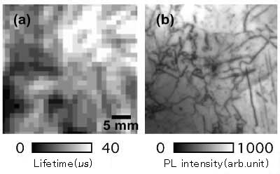
Fig. 4 Defect distribution in multicrystalline Si wafer:
(a) Microwave photoconductivity decay method; 20 minutes in measuring time
(b) PL imaging with wafer immersed in HF solution; 0.1 seconds in measuring time
Meaning of the achievements
The evaluation method for the quantitative measurement of impurities in Si crystals had a great academic influence on the solid-state physics, and at the same time it had extremely great impact on the semiconductor industry. Since the method had epoch-making performance in which a double-digit increase in the sensitivity of detection was achieved as compared with conventional techniques, the technique was immediately adopted by major silicon manufacturers, and it has been settled as an international standard. This technique has been used all over the world for more than 30 years from the time of its invention until the present. Also, innovative techniques utilizing PL have been invented one after another in the evaluation of other major semiconductor crystals at present as well, such as GaAs wafers, SOI wafers, SiC wafers, and multicrystalline Si wafers for solar cells as well, and the evaluation equipment that has been manufactured under license agreements has rapidly propagated among research institutes, crystal manufacturers, and device manufacturers in Japan and overseas. The great number of creative research results as described above that are directly linked with commercialization have greatly contributed to the production of semiconductor materials of higher quality.