The 4th (2004) Yamazaki-Teiichi Prize Winner Semiconductor & Semiconductor Device
High-level Synthesis and Verification on System LSI
| Winner | ||
|---|---|---|
| Kazutoshi Wakabayashi | ||
| History | ||
| Mar. 1984 | B. S., University of Tokyo | |
| Mar. 1986 | M. D., University of Tokyo | |
| Apr. 1986 | C&C Research Labs, NEC Corporation, Kawasaki | |
| Sep. 1993 〜 Sep. 1994 |
Visiting Researcher at Stanford University, USA | |
| Jan. 2004 | Senior Manager, System CAD, System Device Research Laboratories, NEC Corporation, | |
| Present | ||
Reason for award
Research Background
With the scale and complexity of system LSI increasing every year, it continues to be difficult to correctly design multiple types of items in a short time. For everything from the description of LSI specifications to the completion of semiconductor chips, which themselves are products, scrupulous checking and reciprocal cooperation on the engineering level are necessary at multiple phases, including circuit design, operation checking and gate design. All of this requires immense time and an abundance of human resources. In keeping, there has been demand for coherent, high-level technology that enables correct design and verification of LSI chips (hardware) in a short time -- and with a limited number of people.
Candidate's Contribution
Since the mid-eighties, Kazutoshi Wakabayashi has been aware of the importance of high-level LSI design technology. He developed original, integrated design technology for LSI synthesis from a software language (C), which had long been a dream of system LSI designers, and was the first in the world to succeed in its practical application. Although design technology that uses C language is now becoming the main in terms of LSI development methods, His foresight concerning what would become a global trend is particularly noteworthy.
Conventionally, high-level design technology involved massive effort; it was the candidate's ingenuity that led him to focus on C, a standard language for software developers. Mr. Wakabayashi, did not simply express existing concepts in C language but formulated an original leading concept - the first of its kind -- to resolve various issues on the boundary between hardware and software by considering LSI as a whole. He then went on to perfect coherent LSI design technology. His design technology consists of a behavioral synthesis system that automatically synthesizes RTL descriptions from C language descriptions (equivalent to LSI block diagrams), and a group of verification tools; thus, in addition to opening up LSI (hardware) design to software developers, he has contributed substantially to reduced LSI development time and improved LSI quality and reliability.
Globally, as well, there are no other examples of LSI development environments that have been integrated not only in terms of synthesis systems but verification systems, as well. His developments have made it possible to produce hardware -- the LSI chip - with unprecedented efficiency. What made this possible was not merely the development of element technology but also his ongoing efforts and leadership in terms of integration focused on practical application, all of which stemmed from the outstanding quality of his scholarly achievements. He regularly assumes a position of leadership at major related academic conferences domestically and internationally. In addition, some of his results are quoted widely, at home and abroad, as fundamental theses on LSI design technology.
Practical application of his design technology is already underway. Although it will surely become a global trend, with system LSI to become increasingly complex and large in future, expectations for LSI design technology that can handle small-lot/multi kind production will naturally rise, particularly for the development of LSI for digital appliances, which are Japan's specialty. This leaves no doubt about the expansive nature of his achievements.
As described above, his development technology has been rated highly in terms of its originality, technical level, commercial impact, and potential, among other aspects. Originating from Japan, this rare system LSI design technology is a true source of pride for the nation. In keeping, He has been awarded the Yamazaki-Teiichi Prize.
Background of research and development
Advances in semiconductor manufacturing technology have caused the scale and complexity of LSI to increase each year. However, devices equipped with LSI tend to have shorter lifecycles, and there has been demand to reduce the required design period. To counteract increases in complexity and scale occurring each year, the achievement of correct design in less time is an issue common to design engineering in its entirety. In the semiconductor field, however, the pace at which scale and complexity increase is substantially faster than it is in other fields.
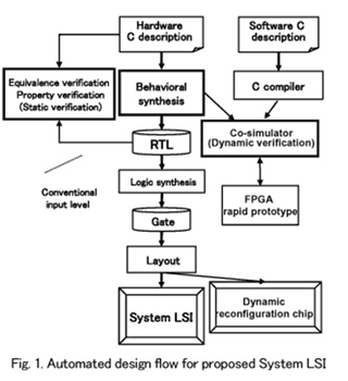
For this reason, improvements in design productivity through the standard efforts to boost design efficiency are not keeping pace with the increasing manufacturing scale. This problem must be overcome by reforming the basic concept of design itself (i.e., the design paradigm). The first wave of reform came in the 70s, with the layout tool (Fig. 1). Circuit design shifted from the use of transistors to the use of AND and OR gates automatically arranged for LSI. Wiring tools were also developed, and design productivity improved rapidly. The second wave of reform occurred in the 80s, with the advent of the logic synthesizer (Fig. 1).
By limiting the type of circuit to the one-phase synchronization circuit used for general-purpose machinery, gate-circuit synthesis tools were developed from descriptions on the block-diagram level (known as RTL) and put to practical use. However, automation of even higher level processes was found to be exceptionally difficult; although many European and American ventures and LSI manufacturers have taken on the challenge since the late 90s, success in practical application has proved elusive.
Achievements
This research achieved automation of LSI design on a higher level than RTL. Methodology derived from behavioral synthesizer tools that automatically synthesize RTL from a general software programming language (Fig. 1) and that derived from a group of verification tools were developed. Compared with the first- and second-generation reforms cited earlier, which transformed the methodology of the world of hardware design, this research has made even more essential reform possible: the reform of methodology that makes hardware design resemble software design. In addition, compilers for the dynamic reconfiguration chip (Fig. 1), heralded as an innovative next-generation chip, were also actualized through this research.
The prizewinner devised a group of algorithms that form the core technology of the behavioral synthesizer; proposed total system LSI design methodology based on it thereafter; developed an integrated design environment from behavioral synthesizers and verification systems; and unified all the facets involved.
Meaning of the achievements
Although behavioral synthesis technology had long been regarded as something of a pastime for researchers, the prizewinner's group tenaciously geared their research and development to practical application. In 1993, they succeeded in the application of manufactured chips, which has led to applications to numerous products at present, including cellular phones and DVD recorders. This system for practical application of behavioral synthesis from C language is the first of its kind in the world. At present, this system alone is being utilized in wide range of design fields, enabling it to lead the world.
The specifics of the effectiveness of the new design methodology proposed are as follows.
- Amount of description necessary for design: With the conventional RTL description, design technology for cellular phone chip design requires about 300,000 lines; with C-language description, it requires around 40,000. This has enabled a conversion from the conventional hardware-type methodology of "connecting circuit components" to software-type design methods of "describing the operations one wants performed". Thus, hardware can now be made for complex processes that it was thought could only be done with processors, owing to the conventional difficulty of making hardware.
- Verification time: Since the simulation speed for investigating design correctness has become dozens of times faster, the result is that what used to take about one week can now be accomplished in several hours.
In keeping, the conventional time required for design has been reduced by half and an improvement of quality on par with the operation of the first manufactured LSI has been achieved.
Henceforth, in addition to low prices and reduced power consumption, the specifics of what intelligent home appliances actually do (i.e., functionality) will become increasingly important. In keeping, this research will likely prove indispensable to having system LSI play a leading role in providing added value, rather than leaving it entirely up to general CPUs.