The 9th (2009) Yamazaki-Teiichi Prize Winner Semiconductor & Semiconductor Device
Pioneering development of seminal low-leakage CMOS circuits
| Winner | ||
|---|---|---|
| Yoshinobu Nakagome | ||
| History | ||
| Mar. 1980 | Completed Masters at Interdisciplinary Graduate School of Science and Engineering, Tokyo Institute of Technology | |
| Apr. 1980 | Entered Central Research Laboratory, Hitachi, Ltd. | |
| Apr. 2003 | Department Manager, Advanced Analog Technology Div., Renesas Technology Corp. | |
| Oct. 2004 | General Manager (current position) | |
| Present | ||
| Winner | ||
|---|---|---|
| Masashi Horiguchi | ||
| History | ||
| Mar. 1979 | Completed Masters at Faculty of Engineering, The University of Tokyo | |
| Apr. 1979 | Entered Central Research Laboratory, Hitachi, Ltd. | |
| Sep. 2000 | Completed doctorate (engineering) at The University of Tokyo | |
| Apr. 2003 | Senior Engineer, Advanced Analog Technology Div., Renesas Technology Corp. | |
| Apr. 2004 | Chief Engineer (current position) | |
| Present | ||
| Winner | ||
|---|---|---|
| Takayuki Kawahara | ||
| History | ||
| Mar. 1985 | Completed Masters at Faculty of Sciences, Kyushu University | |
| Apr. 1985 | Entered Central Research Laboratory, Hitachi, Ltd. | |
| Nov. 1993 | Completed doctorate (engineering) at Kyushu University | |
| Apr. 2005 | Chief Researcher (current position) | |
| Present | ||
Reason for award
The prize winners were the first in the world to announce a number of low voltage basic CMOS circuits, and in particular basic CMOS circuits that reduce increasing MOSFET sub-threshold leakage currents with the lowering of voltages. This was followed by a number of pioneering practical research topics and patents, which have greatly contributed to the semiconductor industry, and the development of high performance nano-scale CMOS LSIs in particular.
During the period between the 1980s and the mid 1990s, all three were the first in the world to discover and develop circuits required for reducing leakage current in low voltage CMOS LSIs. In 1990, Mr. Nakagome lead a team that developed the world¡Çs first, cutting-edge 1.5 V 64 Mb DRAM. This development focused on an operating voltage of 1.5 V while other researches and developments were still in the 5 V, 16 Mb range, and the 64 Mb record was world breaking news at the time. Yet this research was also the first to uncover to the world the leakage current issues that are vital in low voltage CMOS LSIs. The high performance CMOS LSIs using smaller devices with lower breakdown voltage was maintained by lowering the operating voltage (VDD) and lowering the MOSFET threshold voltage (Vth). Yet when Vth approaches 0.4 V, MOSFET sub-threshold leakage current becomes apparent, and increases exponentially as Vth becomes lower. Accordingly, a lower limit exists for VDD (for example 1.5 V), and reduction in the leakage current is essential to lower VDD any further. By the mid 1990s, the winners had discovered and developed the basic concepts for the reduction in leakage current with the use of high-Vth MOSFET power switches, low Vth MOSFET gate/source offset driving, gate/source reverse bias using low Vth MOSFET, and multiple-Vth circuits, which subsequently solved the issue of leakage currents.
The basic circuits that the prize winners discovered and developed formed the beginning of development for subsequent CMOS circuits featuring low voltage and low power. To this day, a large number of reduction circuits have been subsequently proposed, however after careful selection of these circuits, the only practical ones used as the standard technology in the today¡Çs industry are based on the circuit developed by the three winners back in the 1990s. Without this discovery, it would have been difficult to achieve fast CMOS LSIs that use small devices, and in fact, it would have been impossible to produce the latest CMOS LSIs that use devices with dimensions less than 90 nm. By looking at how fundamental and essential this discovery was, it is expected to become extremely useful in low-voltage (under 0.5 V) era using smaller devices.
The basic circuit developed by the prize winners is a revered basic technology that was developed right here in Japan. It has been used widely in the LSI industry for a relatively long period of 20 years, and the value of the technology is well known and treasured around the world. The creativity, spillover effects, impact on industry and society, and the promise that this technology holds are remarkable. Accordingly, the achievements of Mr. Nakagome, Dr. Horiguchi and Dr. Kawahara have been selected as the 9th Yamazaki-Teiichi Prize Winner.
Background of research and development
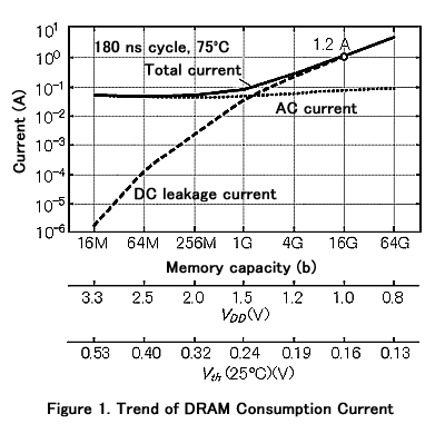
CMOS LSIs are constantly improving in their performance with lower cost while retaining and improving high level of reliability and ease-of-use, and have become essential parts for data communication era of today. With the recent major increases in LSI power dissipation, requirements from more advanced mobile appratus and greater efforts to combat global warming, lower power LSIs are becoming sought after even more. The most effective way of achieving lower power is by reducing the operating voltage according to the device scaling. Yet issues arise when the sub-threshold leakage current increases exponentially as the threshold voltage (Vth) of MOSFETs decreases, making it difficult to produce low power LSIs without incorporating revolutionary new circuitry (Fig. 1).
Achievements
This research was the first to focus on the development of various forms of basic circuitry used to reduce leakage currents and to achieve faster operation at lower voltages. The research can be summarized with the following four basic principles, and have been used as fundamental industrial technologies.
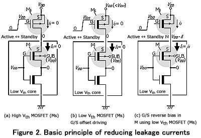
- ¡Power switches consisting of high Vth MOSFETs
MOSFET (Ms) is turned off during standby, the power supply voltage (VDD) is isolated from the low-Vth core (circuit block) and the sub-threshold leakage current (IL) through the core is cut off (Fig. 2(a)). This is used by major MCU/MPU manufacturers in Japan and around the world. - ¢ Gate/source offset driving of low Vth MOSFETs
a high voltage (VDH) is applied to the gate of low Vth Ms, which operates as a power switch, during standby mode. The bias between the gate (G) and source (S) is reversed to make effective high Vth of Ms, and the core leakage current (IL) is cut off (Fig. 2(b)). This concept is widely used as negative word line of DRAMs, and its applications to logic circuits have been reported numerous times at major conferences. - £ Gate/source reverse bias using a low Vth MOSFET
the node N voltage is reduced by the off current (leakage current il) flowing through the low Vth power switch Ms in standby mode. A reverse bias ¦Ä is automatically applied to the gate/source of the MOSFET (M) within the core to reduce the leakage current of M (Fig. 2 (c)). This principle is most effective in DRAM/SRAM iterative circuit blocks. - ¤Dual Vth circuits
combining MOSFETs with low Vth and high Vth, low Vth MOSFETs for logical circuits (critical path) that determine operating speed within the core, and high Vth MOSFETs for the majority of other parts serve to maintain speed and low current leakage within the core. This is a type of circuit that is used widely today, and can vastly reduce the standby current of MPUs.