The 14th (2014) Yamazaki-Teiichi Prize Winner Semiconductor & Semiconductor Device
Development of high-reliability technologies for Ferroelectric Random Access Memory and its mass-production
| Winner | ||
|---|---|---|
| Takashi Eshita | ||
| History | ||
| Mar. 1986 | Completed the latter period of the doctoral course at the Graduate School of Engineering, Nagoya University | |
| Apr. 1986 | Entered Fujitsu Ltd. | |
| Apr. 1996 | Chief researcher, Fujitsu Laboratories Ltd. | |
| Apr. 2001 | Director in charge of FRAM Business Division, Fujitsu Ltd. | |
| Jun. 2006 | Director, FRAM Process Engineering Division, Fujitsu Ltd. | |
| Dec. 2012 | Director, System Memory Business Division, Fujitsu Semiconductor Ltd. | |
| Present | ||
| Winner | ||
|---|---|---|
| Shoichiro Kawashima | ||
| History | ||
| Mar. 1982 | Graduated from the Faculty of Engineering, the University of Tokyo | |
| Apr. 1982 | Entered Fujitsu Ltd. | |
| Apr. 1996 | Chief researcher, Fujitsu Laboratories Ltd. | |
| Apr. 2001 | Director, Memory Device Research Division, Fujitsu Laboratories Ltd. | |
| Aug. 2012 | Deputy General Manager, System Memory Business Division, Fujitsu Semiconductor Ltd. | |
| Oct. 2013 | Senior Director, System Memory Business Division, Fujitsu Semiconductor Ltd. | |
| Present | ||
| Winner | ||
|---|---|---|
| Shigeo Kashiwagi | ||
| History | ||
| Mar. 1979 | Graduated from the Faculty of Engineering, the University of Tokyo | |
| Apr. 1979 | Entered Fujitsu Limited. | |
| Dec. 2001 | Director, Technology Development Department, FRAM Business Division, Fujitsu Ltd. | |
| Jun. 2009 | Corporate Senior Executive, Fujitsu Microelectronics Ltd. | |
| Apr. 2012 | Member of the Board and Corporate Senior Executive Vice President | |
| Apr. 2014 | President & CEO, Fujitsu Electronics Inc. Member of the Board and Corporate Senior Executive Vice President, Fujitsu Semiconductor Ltd. | |
| Present | ||
Reason for award
Ferroelectric memory (FeRAM), which is nonvolatile memory capable of operating at high speed, was actively developed on a global scale in pursuit of the creation of a new market, and more than ten Japanese, U.S., and Korean companies were engaged in the development of FeRAM in the 1990s. Most of these companies, however, pulled out of this business because they failed to resolve the degradation of the ferroelectric characteristic in the manufacturing process. Despite such situation, the candidates developed technology for providing protective film structures with a higher degree of reliability in consequence of scientific scrutinization of the degradation mechanism of the ferroelectric characteristic and, in 1999, succeeded first in the world in the practical application of FeRAM (64kb) operating at 5V. Following the development of new circuit technology, they successfully mass-produced 3.0V operating FeRAM (256kb) in 2003 and 1.8V operating FeRAM (2Mb) in 2007, both of which opened up a market of products that make the most of their high speed and low power consumption characteristics and distinguished writing durability (smart cards, authentication chips, etc.) and registered annual sales of about 10 billion yen at present. FeRAM is expected to greatly expand its market in the fields of the environment/energy and medicine that takes advantage of FeRAM's high γ-ray resistance.
Due to the aforesaid reasons, the three researchers, Dr.Eshita, Dr.Kawashima, and Mr.Kashiwagi, will be an awardee of the 14th Yamazaki-Teiichi Prize in the field of semiconductors and semiconductor devices.
Background of research and development
Smart cards and mobile terminals, which were widely diffused in the 1990s with the sophistication of information and telecommunications technology, required nonvolatile (memory remains even after the power is turned off) memory, which was durable against frequent rewriting, could be rewritten at high speed, and consumed less power, but nonvolatile memory, such as flash memory proliferated at that time, could not meet these requirements. On the other hand, ferroelectric memory (FeRAM) was the optimum memory capable of fulfilling the abovementioned requirements, and many Japanese and U.S. companies attempted to bring it to practical use. However, mass production failed in many cases because the ferroelectric substance was deteriorated in semiconductor processes.
Achievements
The winners presumed that the deterioration of the ferroelectric substance (lead zirconate titanate: PZT), an oxide, was attributable to the reduction induced by the hydrogen produced in semiconductor processes, and tried to elucidate the mechanism of deterioration using deuterium (D2), which has the same chemical property as hydrogen (H2), as tracer. As a result, they were the first to quantitatively reveal that the polarization of the ferroelectric substance decreased when a ferroelectric capacitor was heated to 200℃ or higher in an H2 or D2 atmosphere and 1019 or more H2 (D2) particles entered the ferroelectric substance per cubic meter (Figure 1). To prevent it, they developed a technology for covering ferroelectric capacitors with a protective film impermeable to H2 (Figure 2), and first succeeded in mass-producing FeRAM in the world in 1999.
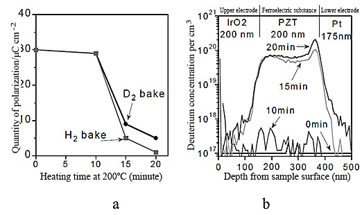
Fig. 1 Deterioration of ferroelectric substance heated (to 200℃) in hydrogen and deuterium (a) and relationship between deuterium concentration in ferroelectric substance (PZT) and heating time (b)
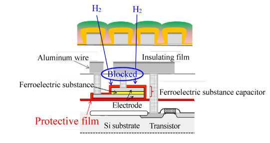
Fig. 2 Cross section of FeRAM. The protective film blocks the ingress of hydrogen from outside.
A storage unit circuit of FeRAM is shown in Figure 3. When reading data, a conventional system applies the voltage to the ferroelectric capacitor by keeping the bit line in the floating (it is not connected to the power supply or ground), bringing the transistor into conduction, and driving the plate line (Figure 3a). In this step, data is detected with the electric charge output from the ferroelectric capacitor as the voltage change of the bit line. Since the power voltage is divided into the capacitor capacity and the bit line capacity, only a smaller voltage than the power voltage can be applied to the ferroelectric capacitor. This made data reading inaccurate and prevented high integration. As a solution to this problem, a terminal circuit and other devices were added to the bit line to artificially use the bit line voltage as ground potential and thereby apply the power voltage to the ferroelectric capacitor (bit line ground sensing system, Figure 3b). In addition, improvements in various circuits and process technologies significantly increased the degree of integration of FeRAM from several dozen kilobits in the early days to the megabit level.
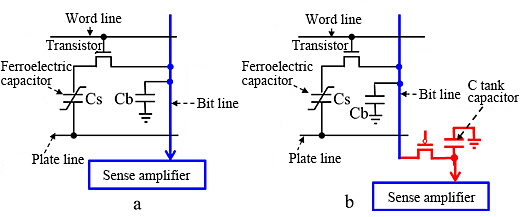
Fig. 3 Storage unit circuit of conventional FeRAM (a) and storage unit circuit of FeRAM adopting bit line ground sensing system (b)
Meaning of the achievements
FeRAM's number of rewriting times, rewriting speed, and power consumption are 100 million times higher (infinite in actual use), about 150,000 times higher, and about 1/10, respectively, than those of flash memory, which is conventional nonvolatile memory. Thanks to these distinguished properties FeRAM opened up a new market (Figure 4). Smart cards and authentication chips using FeRAM ensure an enhanced level of security and provide commercial transactions on the information network, which are an integral part of our daily lives, with higher safety and reliability. We are determined to realize higher integration and cost reduction through further refinement and expand the FeRAM market to the fields of aircraft part control, electronic tags for medical use, etc.
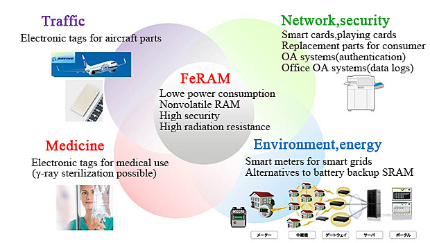
Fig. 4 FeRAM market