The 10th (2010) Yamazaki-Teiichi Prize Winner Material
Technical innovation in ArF resist material for LSI production to 90nm-era and beyond
| Winner | ||
|---|---|---|
| Satoshi Takechi | ||
| History | ||
| Mar. 1980 | Graduated from Department of Chemistry, Faculty of Engineering Science, Osaka University | |
| Apr. 1980 | Joined FUJITSU, LTD. | |
| Apr. 1998 | Project Manager of the Same | |
| Jan. 2003 | Intellectual Property Center Standard Promotion Department of the Same | |
| Apr. 2010 | Joined FUJITSU SEMICONDUCTOR LTD. | |
| Present | ||
| Winner | ||
|---|---|---|
| Koji Nozaki | ||
| History | ||
| Mar. 1986 | Graduated from Department of Chemistry, Faculty of Science, Hokkaido University | |
| Mar. 1988 | Completed Master Course, Graduate School of Science, Hokkaido University | |
| Apr. 1988 | Joined FUJITSU LTD. | |
| Jun. 1993 | Joined FUJITSU LABORATORIES LTD. | |
| May 2002 | Senior Researcher of the Same | |
| Jun. 2008 | Research Fellow of the Same | |
| Present | ||
Reason for award
For microfabrication of a large-scale integrated circuits (LSI), the photoengraving technique (photolithography) is indispensable. For the microfabrication, research and development of a photosensitive materials (photoresists) corresponding to the short wavelength of the light source to be used is necessary. ArF (argon fluoride)lithographic technique using ArF excimer laser with wavelength of 193 nm is shorter than that of conventional light sources was indispensable for LSI fabrication of the 90-nm generation required at the beginning of the 21st century.
Satoshi Takechi and Koji Nozaki proposed a concept of a new material using an adamantyl group for the first time in the world in 1990, while the resist comprising benzene rings which is effective at the wavelength becomes ineffective with the wavelength less than this. Then, a new resist material for ArF excimer laser lithography combining adamantyl groups, lactone groups and the like was put in practical use.
At present, this technique become the world standard, the number of patent citations is quite large. This resist material occupies the market size of 30 billion yen/year or more, in the semiconductor market of about 20 trillion yen, the market of LSIs produced using the resist is estimated to be 10 trillion yen per year.
For the above reason, Satoshi Takechi and Koji Nozaki shall be awarded the 10th Yamazaki-Teiichi Prize in Material.
Background of research and development
Semiconductor large-scale integrated circuits (hereinafter, LSIs) have played the central role as the brain part of electronic devices or systems. Microfabrication of LSIs has been promoted aiming at economical merit associated with miniaturization and high-performance by high integration. The microfabrication has developed by shortening the wavelength of the light mainly used by photoengraving technique (lithography technology). However, for fabrication of 90-nm generation LSI needed at the beginning of this century, a new ArF lithography technology using the ArF excimer laser light (hereinafter, ArF light) of wavelength (193 nm) shorter than before was needed. For the realization, a new material which would replace conventional photosensitive materials (resist) was indispensable. However, there was no prospect of a new resist material and it was the biggest issue of ArF lithography technology realization.
Achievements
This research developed an "ArF resist material", and proposed new material concept different from the convention, proceeding towards practical use.
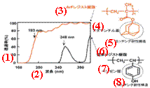
Since resin comprising benzene ring which had been used for resist conventionally was opaque at ArF wavelength of 193 nm, it posed a major problem that it would not function as resist. In addition, benzene rings were indispensable for dry etching resistance which was characteristics needed in an LSI manufacturing process, a new material having transparency and dry etching resistance was required to realize ArF lithography.
The awardees found an alicyclic structure with carbon linked in a circle as a material with both of transparency and dry-etching resistance, and they introduced an adamantyl group which is one type of it into resist to realize compatibility between transparency and etching resistance which was impossible before for the first time in the world (patent applied in 1990).
Fig. 1 Compatibility of transparency and dry-etching resistance
(1) Transmittance (%)
(2) Wavelength (nm)
(3) ArF resist resin
(4) Adamantyl group
(5) Etching resistance structure
(6) Conventional resist resin
(7) Benzene ring
(8) Etching resistance structure
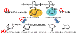
Then, development of ArF resist materials focused on alicyclic structure resin, whose strong hydrophobicity prevented to form fine patterns. The awardees have realized a resist having advanced performance by the technology development below. They developed an oxo ring structure having high hydrophilicity, with which they combined an adamantyl group having high hydrophobicity to enable formation of a high definition pattern (patent applied in 1994). They realized the world's first ArF resist having practical performance by improving solubility of an exposure part in the developing solution by making an adamantyl group acid decomposable (cleavable) for high performance and by using a lactone group having stronger hydrophilicity for an oxo ring structure (patents applied in 1995 and 1996).
Then, they completed a new material concept combining an adamantyl group having an alicyclic structure and a lactone group having the strong hydrophilicity with cost reduction and improvement in the function of the material. In addition, by licensing the technology to resist manufacturers to promote introduction of the developed resist into the LSI manufacturing process, they realized application in leading edge LSI production at the beginning of this century.
Fig. 2 Concept of new ArF resist material
(1) Cleavable adamantyl group
(2) Methyladamantyl group, Mevalonic lactone group
(3) Lactone group
(4) Ethyladamantyl group, Butyl adamantyl group, Hydroxy-γ-butyrolactone group
γ-Butyrolactone group
Meaning of the achievements
This resist material has both high definition resolution and practical etching resistance, as the result of licensing of technology to a resist manufacturer, it was applied to LSI mass production as a standard resist for ArF lithography.
ArF lithography was introduced into production of the prototypes of 90-nm generation LSIs in about 2001 by device manufacturers, and this resist material was used. It was also applied to mass production of 90-nm generation LSIs which got in full swing around 2004. This resist material having high resolution was continuously applied to production of 65-nm generation LSIs (mass production started in 2006) and 45-nm generation LSIs (mass production started in 2008). In addition, this resist material will be continuously used for fabrication of 32-nm generation LSIs whose mass production will be started in 2010. The achievements applied to leading edge LSI mass production since 90 nm has contributed to the low power consumption and high speed of LSIs by microfabrication.
According to the Semiconductor International Capacity Statistics (SICAS), the leading edge LSI manufacturing lines after 90-nm generation occupies about half of the global productivity, It is estimated that the achievements have a ripple effect on the 10 trillion yen market of about 20 trillion yen semiconductor markets according to the World Semiconductor Trade Statistics (WSTS).
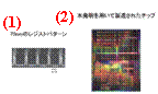
Fig. 3 Pictures of 70-nm resist pattern cross-section and LSI chip manufactured using it
(1) 70-nm resist pattern
(2) Tip manufactured using the present invention