The 11th (2011) Yamazaki-Teiichi Prize Winner Measurement Science and Technology
Development and application of spin-polarized low energy electron microscope for dynamic observation of magnetic domains
| Winner | ||
|---|---|---|
| Tutomu Nakanishi | ||
| History | ||
| Mar. 1973 | Completed Doctor's Course, Graduate School of Science, Nagoya University | |
| Aug. 1973 | Research associate, Graduate School of Science, Nagoya University | |
| Dec. 1987 | Assistant professor, Graduate School of Science, Nagoya University | |
| Apr. 1995 | Professor, Graduate School of Science, Nagoya University | |
| Mar. 2009 | Retired Graduate School of Science, Nagoya University | |
| Mar. 2009 | Emeritus Professor, Graduate School of Science, Nagoya University | |
| Present | ||
| Winner | ||
|---|---|---|
| Yoshikazu Takeda | ||
| History | ||
| Mar. 1977 | Completed Doctor's Course, Graduate School of Science, Kyoto University | |
| Apr. 1977 | Research associate, Faculty of Engineering, Kyoto University | |
| Apr. 1986 | Lecturer, Faculty of Engineering, Kyoto University | |
| Apr. 1990 | Assistant Professor, Faculty of Engineering, Kyoto University | |
| Apr. 1991 | Professor, Faculty of Engineering, Nagoya University | |
| Apr. 2007 | Director, Nagoya University Synchrotron Radiation Research Center | |
| Present | ||
| Winner | ||
|---|---|---|
| Takanori Koshikawa | ||
| History | ||
| Mar. 1974 | Completed Doctor's Course, Graduate School of Engineering, Osaka University | |
| Apr. 1975 | The Osaka Electro-Communication University faculty-of-technology lecturer | |
| Apr. 1977 | Assistant Professor, Faculty of Engineering, Osaka Electro-Communication University | |
| Apr. 1984 | Professor, Faculty of Engineering, Osaka Electro-Communication University | |
| Apr. 2000 | Director, Graduate School of Engineering, Osaka Electro-Communication University (4 years) | |
| Apr. 2003 | Director, Fundamental Electronics Research Institute, Osaka Electro-Communication University | |
| Present | ||
Reason for award
In 2007, A. Fert and P. Grunberg were awarded the Nobel Prize in Physics for the discovery of the giant magnetoresistance (GMR) effect since they exploited a very new "spintronics" field. However, the measurement science and technology necessary for engineering development in this field was not sufficiently prepared.
Three researchers, Nakanishi, Takeda and Koshikawa succeeded in developing a spin-polarized low energy electron microscope enabling real time observation for understanding details of development of magnetic domain that is important for the development of a thin film magnetic material.
With different specialties, they cooperated closely and developed a high-performance spin-polarized electron gun first in the world. The performance was significantly improved in comparison with that of the conventional one, i.e., increased brightness by 10,000 times or more, increased spin polarization from 20% to 90%, and the elongated lifetime of the cathode from current mere 3 or 4 hours to about 2 months. As a result, the acquisition time of the magnetic domain image on a solid surface was reduced to 20 ms / frame equivalent to 1/200 of the current value.
They performed dynamic observation of the magnetizing property of a [CoNi2]y multi-layer film in a growth process using the device and found that the stable magnetic property was achieved with only 4 layers. In addition, they obtained a good international reputation with new findings such as that a [CoNi2] / W (110) film showing an in-plane magnetization property would change to a vertical magnetization status only by vapor-depositing Au of only one-atom layer.
As above, Nakanishi, Takeda and Koshikawa have developed and applied the high-performance spin-polarized low energy electron microscope which enables real time observation necessary for development of new magnetic device, magnetic film materials and the like, thus they shall be awarded the 11th Yamazaki-Teiichi Prize in Measurement Science and Technology.
Background of research and development
Our study has revealed that an electron source combining a mechanism generating spin-polarized electrons by exciting valence electrons of a GaAs semiconductor to a conduction band through absorption of circularly polarized light and a mechanism taking out the polarized electrons from the NEA surface having negative electron affinity into vacuum, possesses excellent potential capacity. Cooperation of accelerator physicists (Nakanishi et al.) and semiconductor physicists (Takeda et al.) showed that high polarization of 90% by changing a semiconductor from bulk GaAs to a strained super lattice film, and high current density over 10 A/cm2 by a method narrowing the band bending area on the NEA surface could be obtained. In addition, degradation of the NEA surface was mitigated by the extreme high vacuum environment on the order of 10-10Pa, enabling continuous use for several weeks.
On the other hand, a low energy electrons microscope (LEEM) allows real time observation of dynamic change of metal surface morphology in a visual field diameter of a few to several 10 micrometers with 10 nm resolution. In Japan, Koshikawa et al. have been engaged in the study and made an effort for its popularization.
Achievements
SPLEEM (spin-polarized low energy electron microscope) using a polarized electron beam in LEEM was put to practical use late in the 1990s enabling observation of a magnetic domain structure, however, a large defect remained present in terms of performance. Since the beam intensity of a conventional polarized electron source was 1/1000 or less compared with an unpolarized LaB6 electron source and at least 4 seconds was needed to acquire even a single image, real time observation was impossible. Research and development aiming to overcome this was started as the Development of Advanced Measurement and Analysis Systems (component technology) Project of JST (Japan Science and Technology Agency) 7 years ago.
We made 2 developments to create a high-intensity 20keV polarization electron gun. (1) As a method minimizing the laser spot for high intensity, by abandoning the conventional type in which laser enters through the electron emission surface, we developed a system in which the laser enters from the rear surface of the cathode crystal and converges on the supperlattice structure. Specifically, we obtained breakthrough improvement by achieving the intensity of 2.0 × 10⁷A/(cm2steradian) which was 10,000 times or more of the conventional and one order of magnitude larger than the LaB6 electron source by converging a parallel laser beam of 3 mmφ to 1/1000 or less, a spot of 1.3 μmφ. (2) Along with this, we developed a new photo cathode to maintain polarization 90% of the conventional one. To begin with, we replaced a conventional GaAs substrate with a GaP substrate transmitting a laser beam having a wavelength of 780 nm, and formed a GaAsP mitigation layer and a GaAs-GaAsP strained super lattice film on it, however polarization was up to 60%. This problem was solved by inserting a 0.5 μm GaAs layer between the GaP substrate and the mitigation layer and thus 90% polarization could be attained.
Fig. 1 shows a picture of the new electron gun using the high-intensity / high polarization electron source loaded on the LEEM microscope.
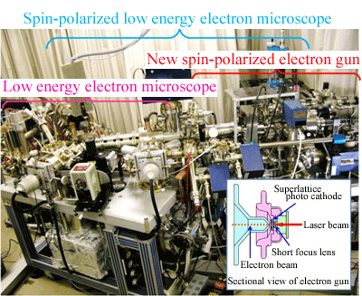
Fig. 1 Entire configuration diagram of SPLEEM microscope
The first experiment of real time observation of the SPLEEM image of the magnetic domain forming process on the Co surface vapor-deposited on the W (110) substrate showed that the image acquisition time was reduced to 20 milliseconds, 1/200 of the conventional one, allowing video recording of 50 frames / second, and thereby the original target was achieved.
Since the direction of the spin of the polarized electron beam can be controlled in any direction, the omnidirectional components of magnetization of a sample can be observed. For example, investigation of in-plane and perpendicular magnetization components of [CONi2] y/W (110) film proposed as a candidate for spin injection (STT) magnetic memory showed that the stable perpendicular magnetization component can be obtained after y=4 stratification. Additionally an investigation of in-plane and perpendicular magnetization components of Au vapor-deposited [CONi2] /W (110) film showed that the single atomic layer of vapor-deposited Au changed its initial in-plane magnetization to perpendicular magnetization as shown in Fig. 2.
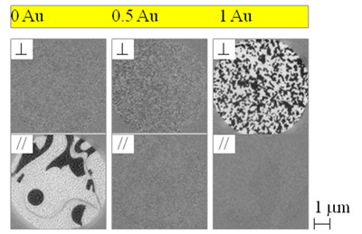
Fig. 2 Observation of Au vapor-deposition on [CONi2]/W(110) film SPLEEM images with the spin of a polarized electron beam directed perpendicular (top) and in-plane (bottom), and Au vapor-deposited in 0 (zero) to one-atom layer
Magnetic domain structure formation in various samples will be investigated in the future, and it is expected that the results will be able to contribute to the development of next-generation magnetic memory.
Meaning of the achievements
Power of the high-intensity / high polarization electron gun developed in cooperation of the researchers in 3 different fields of accelerator, semiconductor and electron microscope has already been internationally recognized in the LEEM and surface-related fields, and there are some order requests placed to them. The commercial production by a company is expected and the JST''s device development project is in progress at present. As for research, it is expected that SPLEEM which is capable of real time observation will advance detailed study of the surface magnetic domain structure forming process that will contribute to the development of new magnetic storage devices. It is also expected that effectiveness of this polarization electron gun as a measurement means for spin property such as transmission electron microscopy and inverse photoemission spectroscopy will be confirmed and popularized in the future.