The 1st (2001) Yamazaki-Teiichi Prize Winner Semiconductor & Semiconductor Device
Pioneer Work for High-Quality Epitaxial Growth of Semiconductor Silicon Carbide and Power Devices
| Winner | ||
|---|---|---|
| Hiroyuki Matsunami | ||
| Affiliation at the time of the award | ||
| Professor, Department of Electronic Science and Engineering, Graduate school of engineering, Kyoto University. |
Background of research and development
Wide-gap semiconductor silicon carbide (SiC) has outstanding property values: about 10 times the electric breakdown field strength, 2 times the saturated electron velocity, and 3 times the bandgap and the thermal conductivity of silicon (Si). Its application to power devices could make them compact and could achieve double-digit reduction of Joule loss during operation compared with Si. In addition, switching loss can be kept to a minimum by high-speed operation. Furthermore, high-temperature operation is possible, which enables substantial advances in making cooling equipment compact as well as streamlining (owing to the switch from water cooling to air cooling and the like). If this technology is applied, the entire structure of power electronics will undergo major change, ensuring effective utilization of electrical energy. Consequently, mitigation of the burden on the environment is expected. Nevertheless, the realization of SiC power devices is obstructed by major issues in terms of the establishment of high-quality-crystal growth technology and device process technology.
Achievements
With the aim of realizing SiC power devices, efforts focused on the establishment of high-quality-crystal growth technology and device process technology, trial manufacture of a basic device, and demonstration of its high performance.
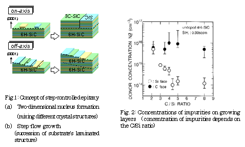
- 1) In 1987, the step-controlled epitaxy method was proposed, making it possible to manufacture high-quality SiC single crystal layers using chemical vapor deposition (CVD), at a temperature lower by 300℃ or more, which previously had not been possible. The basic concept involved the use of a substrate inclined several degrees off from the SiC crystal surface (0001) and the application of step flow growth to easily transmit the substrate's complicated laminated structure to the growth layers (Fig. 1). With crystals to which no impurities were added, a high degree of purity – ppb(10-9) – was obtained (Fig. 2). By adding impurities during growth, a precise conductivity control method was established for p-types and n-types. From various evaluations, not only were the superior aspects of this method demonstrated, through the outstanding crystallinity of the growth layers and the like, but detailed research was done on crystal growth mechanisms and an academic context provided.
- 2) As technology crucial to power device manufacture, a method for local addition of impurities via high-temperature ion implantation was proposed. Annealing conditions were established following implantation, creating the opportunity for opening up the path as a technology to be applied to SiC. The realm of practical use for n-types and p-types is thus approaching.
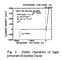
- 3) Using high-quality epitaxial grown layers, low-loss Schottky diodes were produced on a trial basis at voltages of 1kV or above, indicating the possibility of practical use(1993, 1995; Fig. 3). In terms of physical aspects, Schottky barrier height was found to differ due to differences in the polar faces of SiC crystals (the Si and C faces), and the physical basis for this was clarified. These results inspired development aiming for the application and development of semiconductor SiC power devices on global scale. In April 2001, medium- voltage (300V, 600V), low-loss, high-speed Schottky diodes that could not be actualized with Si became commercially available.
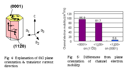
- 4) Where it is optimal for the switching transistor to be the normally-off type where no current is released except during operation, the Power MOSFET (a metal-oxide semiconductor field-effect transistor) is suitable. However, owing to the many defects existing in the SiO2/SiC MOS interface, the electron mobility of the inversion-layer channel becomes extremely small, deteriorating MOSFET characteristics. For this reason, the realization of SiC power MOS transistors had been deemed difficult for the time being. In 1999, using a new crystal plane orientation (11-20; Fig .4) differing from the conventional (0001), MOSFET performance, which had been an issue, was improved around 20 times (Fig. 5), indicating the possibility of realizing Power MOSFET using SiC. As electron mobility has negative temperature dependence, it signifies that as the temperature rises, the current will decrease, making it possible to expect stable operation from power devices. Additional testing at other research institutes has begun. Research on SiO2/SiC interface properties using different plane orientations will likely hasten the actualization of SiC Power MOSFET.
Research Prospects
Establishment of the high-quality single crystal growth technology proposed continues worldwide; thus, low-temperature device processes will be required henceforth. To realize power transistors, thorough understanding and control of the electronic properties of the SiO2/SiC interface will be necessary. Already, low-noise switching power supplies using SiC Schottky diodes are being used. In future, practical research on system aspects will likely expand for inverters for the control of home appliances, automobiles, and industrial motors. With substrate crystal 3 inches in diameter commercially available and crystal defects continuing to be reduced, the realization of high voltage, high-current power devices is comparatively near. SiC power devices will stimulate the development of power electronics, likely inspiring innovation.