The 6th (2006) Yamazaki-Teiichi Prize Winner Semiconductor & Semiconductor Device
Advanced Research for Highly-reliable CMOS Gate Dielectric Films by Direct Nitridation of Silicon
| Winner | ||
|---|---|---|
| Takashi Ito | ||
| History | ||
| Mar. 1969 | Graduated from Dept. of Electronics Engineering, School of Science and Engineering, Tokyo Institute of Technology | |
| Mar. 1974 | Completed Doctoral Course at Graduate School of Tokyo Institute of Technology(Doctor of Engineering) | |
| Apr. 1974 | Joined Fujitsu Limited | |
| Dec. 1989 | Director, Semiconductor Research Div., Fujitsu Laboratories, Ltd. | |
| Apr. 2001 | Head, Silicon Technology Research Laboratory, Fujitsu Laboratories, Ltd. | |
| Apr. 2003 | Chief Scientist, LSI Business Div., Fujitsu Limited⁄Head, Akiruno Technology Center⁄ Chief, Collaborative Research Team of Advanced SoC, National Institute of Advanced Industrial Science and Technology | |
| Aug. 2004 | Professor, Graduate School of Engineering, Tohoku University | |
| Present | ||
Reason for award
Takashi Ito was the first to propose to the world a new process for the direct nitration of silicon for semiconductor device manufacturing. With a range of vanguard application research and patents since then, he has made a tremendous contribution to the semiconductor industry, and particularly to the development of high-performance fine CMOS LSI.
In keeping with advances in MOSFET miniaturization, Mr. Ito foresaw limits to thinning, in terms of reliability, with the conventional thermally oxidized silicon gate films. He proposed a new gate film process: a technology for directly nitridized gate films that would produce even, ultrathin films through the direct reaction of high-purity ammonia gas and silicon. In addition, Dr. Ito verified the outstanding structural fineness, electrical stability and the like. Specifically, he developed a series of technologies that includes substrate cleaning technology that suppresses the growth of native-oxide films on silicon, nitridation gas purifying technology, ammonia gas refineries, furnace equipment for direct nitridation, etching process technology for direct nitridation, and ammonia plasma nitridation equipment that makes a low process temperature possible. Moreover, through research on Si-N binding and how it affects MOSFET reliability and the like, Dr. Ito verified that the silicon nitride films generated are overwhelmingly superior to the conventional thermally oxidized silicon films in terms of chemical stability, the ability to block the penetration of impurities, thermal oxidation resistance, dielectric breakdown resistance, radiation resistance, the suppression of short channel effect, etc. This will enable both the thinning of gate-oxide films and high reliability to be achieved for MOSFET and has made possible the commercialization of CMOS LSI under 90nm-node, the smallest processing dimension, which had been impossible with the conventional thermally oxidized silicon films. Dr. Ito has long published the aforementioned original research results in academic publications and has accelerated the application of silicon nitride films worldwide. In addition to demonstrating such leadership, Dr. Ito is to be particularly noted for his entrepreneurship in establishing the rights to development technologies through the filing of numerous patents.
The range of application for these research results and the pervasive effect of them are extremely large. Since the late 1990s, in addition to the aforementioned gate oxide films for fine MOSFET, it has been practically applied to multilayer dielectric films for capacitors for DRAM of 16Mbits or more (with the percentage of defects 1/10th of what it is for the conventional thermal oxide films), tunnel dielectric films for flash memory (with the number of rewrites improved by one digit or more from what it is conventionally), and the creation of fine element separation. The technology that Dr. Ito developed has become element technology for the manufacture of high-performance fine LSI, at present, beginning with the market for microprocessors and large-capacity memory, and which is valued at over several trillion yen. In the near future, it is expected that this technology will also be applied to high-k gate-oxidized film processing.
In these ways, the technology that Dr. Ito developed can be highly valued for its originality, technical standard, impact on industry, potential and the like; it is indeed an outstanding semiconductor process technology of which Japan can be proud.
Background of research and development
The complementary metal-oxide-semiconductor (CMOS) is a basic structure for the semiconductor devices that support today's information society. Advances in CMOS LSI are striking, with the number of CMOS transistors on silicon chips already exceeding one billion. Such rapid advances in CMOS LSI have been realized through the relentless innovation of semiconductor technology, centering on miniaturization, and advances in the science that supports it. It is no exaggeration to say that the material process aspects have been supported by the ability to thin thermally oxidized silicon films, which are good dielectric films, by means of thermal oxidation. As it had been thought that thermally oxidized silicon gate dielectric films could not be replaced by other materials, their standing was considered firm. However, as ever- thinner dielectric films will be required as transistor miniaturization progresses, it will conceivably become increasingly difficult to achieve both transistor performance and reliability by extending the conventional technology. The necessity of developing highly reliable CMOS gate dielectric films to replace thermally oxidized films was thus anticipated.
Achievements
Noticing possibilities for the utility of technology for the direct nitridation of silicon in the CMOS LSI manufacturing process, the prizewinner promoted vanguard research for it as semiconductor process technology.
In the 1960s, there were a few lab reports on the thermal nitridation of silicon. Although the silicon nitridation reaction occurred at high temperatures over 1300℃, reaction products were characterized by uneven polycrystallization, leading to the conclusion that application to silicon devices would prove very difficult. The prizewinner pursued the cause of this and found it in the residual oxygen or moisture in the nitriding atmosphere. In keeping, they developed various technologies, including silicon wafer cleaning technology that suppresses the adherence of naturally oxidized films; nitrogen gas purification technology that thoroughly removes the oxygen and water that block the nitriding reaction; ammonia gas refineries to generate active nitrides; thermal nitriding furnaces that prevent external oxidized gas from intruding and suppresses degassing; and etching technology for thermal nitride film. In addition, plasma-thermal nitridation equipment with reduced pressures was developed using the active nitride radicals generated with a high-frequency plasma of ammonia. This made it possible to have a lower nitriding process temperature than when plasma is not used. Additionally, in the process of developing technology for the direct nitridation of silicon, it was also discovered that part of the thermally oxidized silicon film itself can also be directly nitridized. In terms of thermodynamics, although even at a high temperature of 1200℃, almost no nitridation of SiO2 will occur. Thermally oxidized silicon films, however, have various structural defects, and it was found that if ammonia is used, the hydrogen generated from it will cause a deoxidization reaction in the weak portion of the oxidized film, causing nitrogen to bond with the dangling bond the silicon atoms generate. In keeping, the generation of finely structured gate dielectric films with thermally oxidized silicon films as their base also became possible.
Directly nitrided silicon films (or nitride-oxide films, more precisely) have various advantages over the conventional thermally oxidized silicon films. Comparison of the values for them reveals that various valuable effects can be obtained with the former, including the fact that it has about twice the dielectric constant, 1.5 times the density, and 1/10,000 the etching speed in buffered hydrogen fluoride solution of the latter. The value for MOS interface state density is close to what it is for thermally oxidized films, and interface structure, which is most important for MOS transistors, is extremely stable. In addition, through the development of a thermal nitride growth-process sequence that conforms to the LSI manufacturing process, its abundant usefulness in CMOS LSI manufacturing was verified, including the ability to block the penetration of impurities, resistance to thermal oxidation, chemical stability, dielectric breakdown resistance, radiation resistance, suppression of MOS transistor short channel effect, etc. These results could not have been achieved with the conventional silicon nitride films built up by means of chemical vapor deposition (CVD) and the like.
Meaning of the achievements
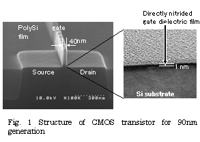
Technology for the direct nitridation of silicon has been emerging in Japan since the late 1970s, and practical application was achieved by subjugating various technical issues. During that time, many research institutes developed derivative and application technologies. Through the accumulation of those technologies, highly reliable CMOS gate dielectric films have come into widespread practical use today. This technology is positioned as indispensable to high-performance CMOS LSI manufacturing, beginning with microprocessors and DRAM in the global semiconductor industry for state-of-the art 90nm generation (Figure 1) and 65nm generation. Henceforth, as well, it will be applied as basic element technology for an advanced information society and conceivably contribute extensively to society.