The 8th (2008) Yamazaki-Teiichi Prize Winner Semiconductor & Semiconductor Device
A pioneer research and industrial development of excimer laser lithography technology
| Winner | ||
|---|---|---|
| Masaru Sasago | ||
| History | ||
| Mar. 1977 | Graduated from Electrical Engineering Dept., Kisarazu National College of Technology | |
| Apr. 1977 | Entered Matsushita Electric Industrial Co., Ltd. | |
| Apr. 1978 | Assigned to Central Research Laboratory, Matsushita Electric Industrial Co., Ltd. | |
| Apr. 1985 | Semiconductor Research Center, Advanced Lithography Project, Matsushita Electric Industrial Co., Ltd., Project Manager | |
| Aug. 1994 | Ph. D., Kobe University Graduate School | |
| Apr. 1996 | Seconded to ArF Lithography Laboratory, Association of Super-Advanced Electronic Technologies (ASET), Research Manager | |
| Apr. 2000 | ULSI Process Technology Development Center, Semiconductor Company, Production Headquarters Matsushita Electric Industrial Co., Ltd., Team Leader | |
| Oct. 2008 | Semiconductor Research Center, Advanced Lithography Project, Matsushita Electric Industrial Co., Ltd., Project Manager | |
| Present | ||
Reason for award
Since its invention in 1958, integrated circuit technology has, over many years, advanced miniaturization, scale enlargement, and high functionality. Serving as the core of technological innovation in many industries, it has major impact on civil life, as well, through the popularization of electronics, infocommunication systems and the like. What has played an important role as one driving force in this development is the advancement of microfabrication technology that centers on optical lithography. Reflecting on the history of optical lithography, although primarily the g-line (wavelength: 436nm) and i-line (wavelength: 365nm) light sources for mercury lamps had been used in mass production, when integrated circuit pattern dimensions were miniaturized to around 0.3μm, the resolution limit was reached and therefore, light sources of even smaller wavelengths started to be in demand. Under such conditions, at the 1986 International Electron Devices Meeting (an international conference), Dr. Sasago proposed lithography technology using the world's first practical krypton fluoride (KrF) excimer laser (wavelength: 248nm) as a light source. Although diversification that combines outstanding element technologies is particularly emphasized in lithography technology, what Dr. Sasago proposed was not only a light source but an integrated processing technology involving exposure devices, resist materials, and the process technologies for mastering their use. Thereafter, Dr. Sasago continued to shorten light source wavelengths and also made an important contribution to realizing lithography using argon fluoride (ArF) excimer lasers (wavelength: 193nm). In combination with numerous technologies for improving resolution that were proposed thereafter, the short wavelength optical lithography technology that Dr. Sasago constantly advanced has become the sole practical technology for the current 45nm technology node generation, as well.
In addition to the successes that were based on his ongoing practical, visionary research, the leadership that Dr. Sasago has demonstrated in this field deserves special mention. Association of Super-Advanced Electronics Technologies (ASET) was established in 1996 in Japan; as the chief of the ArF excimer laser lithography laboratory, Dr. Sasago expanded technology pertaining to the ArF excimer laser lithography that had been proposed to that time and contributed immensely to the practical application of laser lithography, for Japan and for the world.
In these ways, with enthusiasm and determination, Dr. Sasago pulled along the development of the diversified technology that became the core of lithography technology. In consideration of Dr. Sasago's major contribution to the promotion of collaborative development systems in the semiconductor industry, as well, he has been awarded the Yamazaki-Teiichi Prize in Semiconductors and Semiconductor Devices.
Background of research and development
The semiconductor industry continues to expand, driven by semiconductor microfabrication technology, and has come to exert the greatest pull on the electronics industry boom. Personal computers, cellular phones and digital consumer appliances have been successfully produced as a result, leading to the advent of the realization of a ubiquitous society. The greatest technology involved is the shortening of the wavelength used in optical lithography exposure, and many institutes for advanced research throughout the world have taken on this challenge in their research and development.
Achievements
This research constitutes groundbreaking development for excimer laser lithography technology, which has had the greatest impact on such progress. In 1986, a world-leading genuine KrF excimer laser (248nm) was developed around the same time as it was at Bell Telephone Laboratories in the US. Similarly, in 1989, the world's first ArF excimer laser (193nm) was developed. In 1998, the possibility of next-next generation VUV (153nm) lithography for the 100nm generation was announced. Since 1996, commercial production of sub-250nm KrF excimer lasers has been realized and prospects established for mass production technology for sub-90nm ArF excimer lasers. The trend of that technology has become the source of immersion lithography technology industrialization for ArF excimer lasers on the sub-45nm level, which is currently the leading edge (Fig. 1).
The most important factors in advances in miniaturization for optic lithography are shortening the exposure wavelength and increasing the numerical apertures for lenses. This research has its origins in a concept based on the world's first excimer laser exposure done with a simple optical system in 1980 by Toyoda and Namba et al.
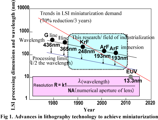
For the purpose of industrialization, the prizewinner focused on shortening the wavelength by means of reduced projection exposure, the basis for which was the application of a monochromatic excimer laser light source. With the excimer laser light source, additional shortening of the wavelength is possible, depending on the gas species. This made developments possible for KrF (248nm) and ArF (193nm). This research covers a wide range for lithography technology as a whole, ranging from exposure devices to resist materials to processes. Not only does this constitute leading research in academia and industry but a patent has been filed for the pattern formation method based on the excimer laser lithography technology that the prizewinner invented, which overcomes the tradeoff in the light absorption of resist materials, owing to the shortening of the exposure wavelength. It will have long-term effects on ArF immersion lithography, for which the sub-45nm level is currently the leading edge.
Meaning of the achievements
Despite apprehension that advances in semiconductor microfabrication technology would be saturated with optical lithography, it is no exaggeration that what made the roadmap for microfabrication (which embodies the ambitions of the international semiconductor industry) definite was no less than these advances in excimer laser technology. Even the latest roadmap predicts that excimer laser lithography technology will still be in use as of 2016. Not only have the prizewinner's conference presentations and article publications to the present time exceeded 200, but he has established special international conferences and deepened technical exchanges with researchers from around the world. At the expert committees of International Technology Roadmap for Semiconductors and other international conferences, he has consistently represented Japan from a position of leadership and has gained standing as a global authority in the field of lithography technology.
Through the development of excimer lithography (KrF→ArF→ArF immersion), mass production commercialization plans will be established for the world's semiconductor industry from 250nm to the 32nm rule. The 65nm to the 40nm level is already used for the industrialization of leading-edge semiconductor LSI for DRAM, Flash and other types of memory, MPUs and system LSI for digital consumer appliance. Henceforth, it is expected to make substantial economic contributions to industry as a basic process technology in the semiconductor industry.