The 10th (2010) Yamazaki-Teiichi Prize Winner Semiconductor & Semiconductor Device
Pioneering research and longtime contribution for industrial approach on extreme ultraviolet lithography
| Winner | ||
|---|---|---|
| Hiroo Kinoshita | ||
| History | ||
| Mar. 1974 | Completed Graduate School of Engineering, Keio University | |
| Apr. 1974 | Joined Musashino Research and Development Center, NTT | |
| Jul. 1993 | Leader of X-ray Reduction Group, LSI Laboratory, NTT | |
| Sep. 1995 | Quit LSI Laboratory, NTT | |
| Oct. 1995 | Professor of Laboratory of Advanced Science and Technology for Industry, Himeji Institute of Technology (Renamed University of Hyogo in April, 2007) | |
| Present | ||
Reason for award
Hiroo Kinoshita proposed the world's first extreme-ultraviolet lithography (EUVL) technology in 1986. Kinoshita, based on strong belief and strong leadership, has consistently made significant contributions to development of this technology by pioneering research and practical application research on EUVL for 25 years. Namely, such as the reduction exposure system using a multilayer film reflecting optical system, an optical system comprising an aspheric reflection mirror and a method for oblique-incidence to mask, reflecting mirror and reflective mask using Mo/Si multilayer, mask fabrication and inspection, as well as various resists etc., he proposed and demonstrated various element technologies or systems related technologies.
EUVL is regarded as the candidate to be the last lithography for microfabrication of semiconductors. The exposure tool, as a mass production level prototype (using Kinoshita's original technology) is globally introduced in the second half of this year; a mass production model will be shipped in two to three years. It is also expected that the related technology development towards practical application of fine semiconductor devices of 20 nm or less also will be advanced quickly.
Without Kinoshita's foresight, originality, and leadership over long period of time, manufacture of fine semiconductor device of 20 nm or less is impossible, his contribution to the semiconductor industry in the world, and his contribution to the related peripheral device industries (light source, resist, mask, etc.) which are specialties of Japan are unfathomable. Since it is the result of world-class large-scale research unique to Japan, Kinoshita shall be awarded the 10th Yamazaki-Teiichi Prize in Semiconductor and Semiconductor Devices.
Background of research and development
With a progress of the information society, supply of compact semiconductors with large capacity became essential, and the progress and the innovation of microfabrication technology which might related to this were desired. In early 1980s, the soft X-ray proximity lithography was regarded as promising, and this method was excellent in resolution, however, preparation of a mask with large exposure area was difficult. Although the conventional ultraviolet exposure method (light source wavelength of 248 nm) was capable of reduced exposure using a refracting optical system , with regard to further microfabrication, the wavelength of an exposure light source or the optical material which constitutes an optical system has a limit (the limit at the time was the pattern line width of 100 nm), thus, it was considered that the demand of the next-generation semiconductor (100 nm or less) might not be met. From such a situation, the grope for an exposure method to meet the requirements (reduced exposure, bulk mask, and capable of covering several generations) of next-generation lithography was begun.
In Japan, Kinoshita proposed the reflection type reduction lithography using extreme ultraviolet (EUV) as a light source, and he succeeded in 4 micron pattern formation at the reduction ratio of 1/5 by a reduced exposure experiment in 1986.
On the other hand, in the U.S., research aiming at 0.1 micrometer was promoted over almost the same period because the U.S. could not exceed Japan in mass production technology of 0.5 to 0.2 micrometer semiconductors. Ceglio et al of LLNL proposed a reflection reduction optical system with light source wavelength of 4.5 nm in 1988. The mask was made a concave spherical surface to avoid curvature of field. In addition, AT&T investigated 1/20 reduced exposure with light source wavelength of 36 nm in 1990, and proposed a system in which the reflecting surface was made of iridium (Ir).
Achievements
Generally, an exposure tool consists of a light source, a reduction optical system, a mask and a resist, Kinoshita presented original proposals for each of them and advanced experiment and demonstration towards practical application.
To meet three exposure conditions of lithography, using the light source of the wavelength of 13 nm, he proposed a reflective optical system with an aspheric surface mirror and a reflective mask in which Mo/Si multilayer coated in 1989.Generally, an exposure tool consists of a light source, a reduction optical system, a mask and a resist, Kinoshita presented original proposals for each of them and advanced experiment and demonstration towards practical application.
To meet three exposure conditions of lithography, using the light source of the wavelength of 13 nm, he proposed a reflective optical system with an aspheric surface mirror and a reflective mask in which Mo/Si multilayer coated in 1989.
The present extreme ultraviolet exposure system (EUVL) was based on this proposed structure. Fig. 1 shows the configuration of the present exposure system.
The present extreme ultraviolet exposure system (EUVL) was based on this proposed structure. Fig. 1 shows the configuration of the present exposure system.
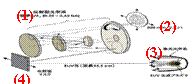
Fig. 1 Outline of EUVL exposure device
(1) Reflective optical system Magnification 1/4 (0.25 - 0.45 NA),
(2) 300 mm wafer
(3) Condensing optical system
(4) Reflective mask EUV light (wavelength: 13.5 nm) EUV generation plasma
The outlines of main proposals are described below.
- ¡ Selection of exposure wavelength
Comprehensively considering resolution against the short wavelength light source, the exposure depth in resist, reflectivity of multilayer, etc. in a reflective optical system, the exposure wavelength was set at 13.5 nm beyond - ¢ Proposal of aspheric reflection mirror optical system
He devised an optical system comprising an oblique-incidence system to the mask and two aspheric surface mirrors to meet telecentric property as an optical system for exposure. This proposed structure is the design principle of the present six-sheet aspheric reflection mirror optical system. In addition, he developed a highly accurate mirror in collaboration with U.S. Tinsley Co., and succeeded in pattern formation in the area of 10 mm x 12.5 mm (large area exposure) in 1995. - £ Proposal of reflective mask
Since manufacture of a transmission type mask in the EUV region is difficult, Kinoshita devised a reflective mask having Mo/Si multilayer as same as a reflecting mirror surface coated on a mask substrate. -
¤ Proposal of two layer-structure resist and chemical amplification resist
¡¡Since the absorption of EUV was too strong with the conventional PMMA resist, he proposed the two layer structure of Si containing resist (SPP) and OFPR. In addition, since PMMA was low sensitivity, he proposed the chemical amplification resist which could be expected of even higher exposure sensitivity.
Since 2002 when development of the above exposure system was settled for the time being, studying the defect inspection method of mask used for EUVL (Stage I CREST), he has constructed a bright field observation system capable of observing both the absorber pattern of a mask and phase defects of mask blanks, and succeeded in observation of the 100 nm absorber pattern and the 20-nm phase defect. Furthermore, he started in 2008, development of a next-generation lens-less system capable of detecting 25 nm defect (Stage II CREST 2008-2013).
On the other hand, he has evaluated outgas from resist in collaboration with a resist company since 2001, and proposed a material with less carbon contamination. In 2010, he built an interference exposure system enabling development of less than 22 nm generation resist in future in the undulator beam line of New Subaru, and succeeded in fabricating 17 nm L&S pattern so far.
Thus, he has contributed to improvement of infrastructure ranging over all lithography technologies for practical application of EUVL.
Meaning of the achievements
It is no exaggeration to say that microfabrication of semiconductors depends on the lithography technology. As a fabrication technology which can accommodate to next-generation semiconductors, Kinoshita has proposed extreme ultraviolet lithography (EUVL) the first in the world, demonstrated the possibility of high resolution and large area exposure while developing a prototype of the EUV exposure system using the technology, and has promoted practical application of EUVL as a world leader in this field.
The ripple effect of the result of research by Kinoshita is very large, besides citation in home and abroad, EUVL is considered as super minute patterning and the memory mass production technology to the limits of next-generation Si devices having pattern line width ranging 32 nm to 22 nm and 16 nm nowadays, research and development have been conducted by research institutions and companies of semiconductor devices in the world. Based on the results of institutions, Moore of Intel estimated that " Moore's principle" could be assured by EUVL in 2002.
In addition, the pattern was compared with that of the conventional ArF immersion exposure, and superiority of EUVL was demonstrated. Reviewed in the cost aspect, it is superior in respect of prices compared with the ArF immersion exposure method and double patterning using it, and early practical application is expected.
With proposal of the innovative lithography by "exposure with the reflective optical system using EUV light", he realized patterning at the level of 40 nm which was impossible by the conventional exposure method, and promoted the semiconductor industry towards practical application of the EUV exposure system. Thus, his achievements are large. In addition, promoting pioneering research on mask and resist as well as system development, he is still making significant contributions to infrastructure construction of future semiconductor mass production technology.
As described above, he proposed the innovative lithography in semiconductor fabrication, and contributed to lead to practical application.