The 11th (2011) Yamazaki-Teiichi Prize Winner Semiconductor & Semiconductor Device
Invention and development of "fin" structure MOSFETs
| Winner | ||
|---|---|---|
| Digh Hisamoto | ||
| History | ||
| Mar. 1986 | Completed Master's Course, Graduate School of Engineering, the University of Tokyo | |
| Apr. 1986 | Joined Central Research Laboratory, Hitachi, Ltd. | |
| Oct. 1997 | Visiting Industrial Fellow, University of California at Berkeley | |
| Oct. 1998 | Senior Researcher, Central Research Laboratory, Hitachi, Ltd. | |
| Jul. 2003 | Received Ph. D. in Engineering from the University of Tokyo | |
| Apr. 2010 | Seconded to Hitachi Research Institute | |
| Apr. 2011 | Returned to Central Research Laboratory, Hitachi, Ltd. | |
| Present | ||
Reason for award
Digh Hisamoto invented the world's first three dimensional fin structure MOSFET (originally named DELTA) to solve the problems related to size reduction of MOSFETs which were being revealed in the second half of the 1980s, demonstrated its effect by fabricating devices with gate length of about 300 nm for trial, and presented it at IEDM (International Electron Devices Meeting) in 1989. Since this structure can suppress the variation in the threshold voltage and the leak current due to the short channel effect of the MOSFET, and furthermore is possible to increase the driving current by increasing the height of the fin, it is suitable for size and voltage reduction. Subsequently, he developed MOSFETs with gate length of 17 nm through the joint research with University of California, Berkeley (UCB), demonstrating possibility of size reduction, and he presented it at IEDM in 1998. Today, the structure is broadly called FinFET representing its shape well.
While the mood for utilization of fin structure MOSFET including LSI (DRAM) for memory has been growing in these years, a logic LSI (MPU) manufacturer has announced that they would commercialize the technology (in the second half of 2011) very recently. These movements indicate that the plane structure MOSFET used over the past 40 years is at a turning point changing into a three-dimensional structure. With the fin structure MOSFET invented and developed by Hisamoto, the size of MOSFET will be reduced continuously henceforth, thus, its contribution to the development of the semiconductor industry is very significant. The research result is very excellent in originality and foresight as well as impact on the industry.
For the above reason, Digh Hisamoto shall be awarded the 11th Yamazaki-Teiichi Prize in Semiconductor and Semiconductor Devices.
Background of research and development
Ultra large-scale integration of semiconductor devices (ULSI) are used for various products such as portable devices, household appliances and cars including the computer, being one of the generic technology supporting our modern life. As to ULSI, there is an empirical rule called "Moore's law", i.e., "Size reduction of a device and exponential increase of integration number will improve performance dramatically". As the result of continuous device size reduction over about half century according to this law, micro fabrication of 20 to 30 nm size and insulation layer formation with film thickness of 1 nm have become necessary. There, various critical physical phenomena such as short channel effects and quantum effects have come to surface, which made it difficult to continue performance in improvement by the conventional scaling rule.
Achievements
Hisamoto invented "fin structure MOSFET" which will be important for growth of the semiconductor industry in the future and demonstrated its effect. With this invention, a "double gate" structure effective in controlling the short channel effect which is a challenge with the conventional planer MOSFET, can be created by a self-aligning micro fabrication process. Fig. 1 shows a bird's-eye view and an electron micrograph of the device.
It is a double-gated structure in which the gate electrodes control the potential in the channel by applying an electric field effect from both sides of the fin structure channel.
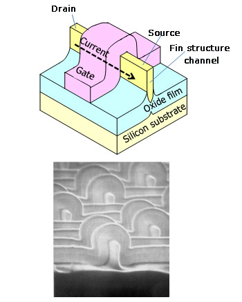
Fig. 1 Fin structure MOSFET (DELTA) (Top)
and electron micrograph of the prototype device (Bottom)
According to the conventional scaling rule, it was necessary to increase the impurity concentration of the channel to suppress the short channel effect for promoting size reduction of MOSFET, resulting in degradation of carrier mobility and threshold variation of a transistor.
Since the double gated structure can control the short channel effects by the electric field effect of the gate, size reduction can be carried out while keeping the impurity concentration of the channel low. However, there was a problem that the planer processing technology currently used in ULSI was not suitable for forming a "gate-channel-gate" layered structure necessary for the double-gated structure. So, Hisamoto conceived to form a channel part in a film "fin" vertical to the wafer surface and realized the first practical double gate MOSFET.
In addition, there was a problem of the current drivability weakening with the size reduction since the MOFSET current drive was dependent on the channel width. In the fin structure channel, since the channel width can be increased by making the fin higher, the channel width can be expanded without increasing the chip area. Moreover, the wide channel at this low concentration is effective to suppress the "threshold voltage variation" revealed in MOSFET size reduction. Therefore, scaling of the device can be easily proceeded compared with conventional planer MOSFET.
Meaning of the achievements
The fin structure MOSFET is a device in which the short channel effects are suppressed to improve properties such as current drivability and threshold voltage stability by incorporating a three-dimensional structure to the channel. It has an advantage of being realizable by conventional planer processing technology unlike other three-dimensional devices. A device named DELTA was presented at an international conference in 1989 and gained widespread attention prolonging the scaling of a planer device. Especially, following the demonstration of scalability down to 20 nm using this structure and the presentation at an international conference in 1998, domestic and overseas universities and research institutes and semiconductor companies have reported many results of research regarding fin structure MOSFET. Through the presentation, various variations were devised for a gate shape etc. and named such as FinFET, Tri-gate, MugFET, Pi-gate, Omega-FinFET and Saddle-FinFET. Since any structure has a fin-like channel, they can be named "fin structure MOSFET" collectively.
For a logic chip, it has been considered to introduce a fin structure to improve computing speed with the high mobility property of a low-concentration channel. In the Semiconductor Roadmap (ITRS: International Technology Roadmap for Semiconductors) in 2010, it was predicted that the fin structure MOSFET (described as "MG [Multi-Gate]" in the table of ITRS) would be used since 2015. However, a U.S. semiconductor manufacturer announced that they would market launch their products using the fin structure MOSFET in 2011 by moving the roadmap forward. This may be because introduction of the fin structure MOSFET was strongly demanded to realize both scale reduction and supply voltage that has been difficult due to threshold voltage variation.
On the other hand, to increase integration degree, it has been considered to use a fin structure to promote size reduction of a memory chip in which reduction of the cell area is important. Based on conference presentation by semiconductor memory manufacturers, introduction of a fin structure MOSFET to DRAM at the 30 nm node (processing dimension of 30 to 39 nm) in 2012 is being expected.
Thus, for the semiconductor industry in the future, performance improvement based on the "Moore's law" will be able to be maintained by replacing the conventional planer MOSFET with the 3 dimensional ones in both the fields of logic/memory chip.
Because the fin structure MOSFET can reduce the supply voltage significantly compared with the conventional device, it may promote reduction of power consumption of various products. While energy issues are being highly focused on, it is expected that new applications requiring low power will be produced by using the fin structure MOSFET.