The 12th (2012) Yamazaki-Teiichi Prize Winner Semiconductor & Semiconductor Device
Pioneering contributions to understanding of carrier transport properties in channels of Si MOSFETs and to technology of the channel mobility enhancement
| Winner | ||
|---|---|---|
| Shinichi Takagi | ||
| History | ||
| Mar. 1983 | Finished the doctorate programs of the Graduate School of Engineering of the University of Tokyo | |
| Apr. 1983 | Joined the Research and Development Center of Toshiba Corporation. | |
| Aug. 1993 | Visiting researcher at Stanford University | |
| Apr. 1995 | Chief Researcher at the Research and Development Center of Toshiba Corporation. | |
| Aug. 2001 | Held concurrently the post of the group leader of the Semiconductor MIRAI Project "New Structure Transistor and Measurement&Analysis Technology Group. | |
| Dec. 2003 | Professor at the Graduate School of Engineering of the University of Tokyo | |
| Present | ||
Reason for award
Dr. Shinichi Takagi is one of the few researchers who have had great influence in the world in researches related to the achieving of higher mobility of MOSFETs consistently from the latter half of the 1980s until the present. Namely, in 1988 Dr. Takagi studied the carrier transport characteristics in the inversion layer that govern the speed of MOSFETs from both aspects of experiment and theory systematically and comprehensively, and on the basis of this study he not only provided guidelines for the method of evaluation of the mobility of scaled MOSFETs and the achieving of higher mobility, but also enabled the building of device models having high universality and usability. The mobility model he advocated has now been incorporated in many commercially available simulators, and it has enabled prediction of the performance of scaled MOSFETs whose prototyping has increasingly become difficult, thereby making great industrial contributions as well. Moreover, in the mid-1990s Dr. Takagi elucidated the physical origin of improvement in mobility of strained-Si MOSFETs for the first time from both aspects of experiment and theory, and the contribution of such elucidation to the design of optimal strained-Si MOSFETs structure that started in around 2003 can be shown from the fact that his relevant papers are widely cited throughout the world. Also, on the basis of this elucidation, he has been continually advocating concepts that improve mobility, and through application of such concepts to varied new-structure MOSFETs such as thin-film SOIs, he has become the driving force in this field.
Dr. Takagi's numerous papers and lectures (158 cases) in international societies as well as conspicuous awards are proof that shows his originality, vision and leadership, and are internationally well known already. Because his researches have a highly balanced focus on experiment and theory, and besides are full of practicality and have high universality, it is thought that they will play an important role in the upgrading of high mobility channel MOSFETs continually from now on.
As stated above, by evaluating the greatness of his social influence on academia and industry through fundamental research, Dr. Shinichi Takagi will be an awardee of the 12th Yamazaki-Teiichi Prize in the field of semiconductors and semiconductor equipment.
Background of research and development
Ultra Large Scale Integrated semiconductor circuits (ULSIs) have realized changes toward higher performance and higher functionality through miniaturization of devices for a long period of more than 50 years. The base of such technological development has been formed by achieving higher current drive of Si MOS transistors that are the constituent elements of ULSIs. One of the important physical quantities that determined the drive current of Si MOS transistors is the carrier mobility of Si in the inversion layer that becomes the channel. Due to this fact, in order to improve the drive current of MOSFETs, it has become extremely important to clarify the physical origin that determines the channel mobility, thereby building its quantitative model, and at the same time to propose and establish engineering techniques that enable the channel mobility to be improved.
Achievements
In this study, in view of the importance of the channel mobility of MOSFETs, the mobility of electrons and holes in the inversion layer of Si MOSFETs was investigated experimentally and systematically by changing the vertical electric field, substrate impurity concentration, temperature, surface orientation, etc. on the MOS interface, whereby the characteristics of the mobility were clarified. As a result of this, as shown schematically in Fig. 1, it has been clarified that it is possible to describe the channel mobility in a unified manner as the "universal mobility" by using the physical quantity of effective electric field Eeff which is the average vertical electric field on the MOS interface, and at the same time the physical origin of the determination of mobility has been successfully clarified quantitatively.
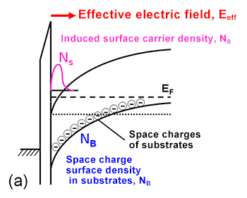
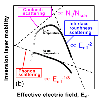
Fig. 1 (a) Schematic band diagram of Si MOS interface
(b) Schematic of the dependency of mobility on effective electric field
and of the scattering mechanism that determines the mobility
The carriers in the Si MOS inversion layer are strongly confined on the MOS interface, and it is known that they have a structure called two-dimensional sub-band. In particular, electrons in the inversion layer on the surface of Si (100) are in two electronic states that are called the two-fold degenerate valleys and four-fold degenerate valleys. In this study, sub-band structure modulation technology has been proposed on the basis of the above characteristics, in which, as an engineering technique for improving mobility, as shown in Fig. 2, the current drive of MOSFETs is improved by lowering the energy level of the electronic state of the two-fold degenerate valleys having excellent characteristics of electric conductivity to a lower level than that of the four-fold degenerate valleys and by increasing the number of electrons in the two-fold degenerate valleys. This structure modulation can be realized by applying tensile strain to the Si channel. The physical origin of improvement in the electron mobility in the MOS channel when applying this strain has successfully been explained quantitatively from the viewpoint of the sub-band structure modulation. Also, as a different sub-band structure modulation method, a method for improving mobility has been proposed in which the confining energy for the four-fold degenerate valleys will be increased by making the Si film thickness extremely thin in the device structure called the SOI (Si-On-Insulator), thereby increasing the confining energy of the four-fold degenerate valleys, and theoretical analysis has been made and at the same time the method has been theoretically analyzed and demonstrated.
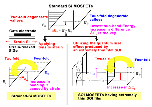
Fig. 2 Schematic of sub-band structure modulation technology in the Si MOS inversion layer
Furthermore, a strained-SOI device structure (Fig. 3) was proposed which combines improvement in mobility resulting from strain with the SOI structure that is a device structure fit for miniaturization, and the excellent characteristics of device operation and of CMOS circuits that are composed of Si MOSFETs were demonstrated by taking a leading part in the world.
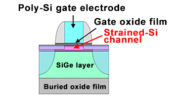
Fig. 3 Illustration showing the cross-sectional structure of a strained SOI MOSFET
Even after that, a study of MOS transistor technology is continued that uses Ge having small effective mass or a III-V compound semiconductor as the channel on the basis of a physical understanding of the mobility of the MOS inversion layer and sub-band structure toward the realization in future of MOS transistors having high current drive.
Meaning of the achievements
The "universal mobility" that has been obtained in this study is widely utilized internationally as data that serve as reference concerning the mobility of Si MOS transistors and also as a basic framework for understanding the physical mechanism of the mobility of Si MOS inversion layers, and at the same time it is generally used as a physical model of device simulators as well.
In addition, with the physical limit of the material properties of Si, in 2000 and thereafter, an impasse of the miniaturization technology of MOSFETs has been recognized, and technologies for improving the mobility of MOSFETs, in particular, strained-Si channel technologies have been examined seriously. In this study, analysis and demonstration of strained-Si MOSFETs were started before activation of the research and development of strained-Si channels in the industry, whereby the mechanism of improving their mobility was clarified, and at the same time through demonstration of the circuit operation of strained-SOI MOSFETs and strained-SOI CMOS by taking a leading part in the world, etc., great contributions have been made to the commercialization of strained-Si technologies.
Also, knowledge that has been acquired in the Si channel is being developed, and research & development of MOS device technologies are continued in which Ge and III-V compound semiconductors are used on which focus is attention as the MOSFETs in the future, and thus contributions are made to the development of device technologies toward the realization of ULSIs in the ultra-miniaturized generation.