The 13th (2013) Yamazaki-Teiichi Prize Winner Semiconductor & Semiconductor Device
Development of Image Sensors with Pinned Photodiode
| Winner | ||
|---|---|---|
| Nobukazu Teranishi | ||
| History | ||
| Mar. 1978 | Master degree of Science, University of Tokyo | |
| Apr. 1978 | Joined NEC Corporation | |
| Jul. 1995 | Manager of the Sensor Research Department of the Microelectronics Research Laboratories of the corporation | |
| Apr. 2000 | Principal Engineer at Matsushita Electric Industrial Co., Ltd. (now Panasonic Corporation) | |
| Apr. 2001 | Group Manager of the CCD Business Division of the Semiconductor Company of the corporation | |
| Jun. 2013 | Professor at the University of Hyogo and Shizuoka University | |
| Present | ||
Reason for award
Nobukazu Teranishi has been engaged in research and development of solid state image sensors (CCD image sensors and CMOS image sensors) for 35 years since 1978 until the present. The 1970s saw expectations of CCD image sensors as image sensors for consumers due to their excellent mass productivity and capability of weight reduction because they can be produced by means of semiconductor technology, but it was a difficult time immediately before commercialization due to problems such as the existence of the image lag, white defects caused by dark current, and also the occurrence of blooming and smear when photographing a high luminance object.
He found out the image lag in CCD image sensors, and clarified its mechanism based on the operating principle of the device having a conventional structure. He proposed the pinned photodiode technology, where the surface of photodiode is covered with a P+ layer having a high impurity concentration. By means of this, not only the image lag but also readout noise were removed by complete charge transfer. The P+ layer realized the low dark current as well as white defect reduction. Besides he also succeeded in suppressing blooming and smear by the invention and proposal of vertical overflow drain (VOD) structures and precise light-shield structures. These results were widely adopted in relevant industries and promoted miniaturization of pixels, thereby opening up the megapixels era and contributed to the widespread use of HDTVs and digital cameras. After the year 2000, with the advancements in LSI technologies, there was the rise of CMOS image sensors with pinned photodiodes which were used in cameras for cellular phones. Moreover, it enabled high resolution photography exceeding 10 megapixels and high-speed photography, and various image-related products and application industries that use a smart phone camera, etc. appeared. In 2012, 2.8 billion image sensors were produced annually, and pinned photodiodes were adopted in almost all the image sensors. It is expected that there will be a wide range of applications including new applications to be developed from now on. The pinned photodiodes proposed and demonstrated by Teranishi are rich in creativity and foresightedness and made a great contribution to the development of semiconductor industries, thus having extremely great ripple effects.
Due to the aforesaid reasons, Nobukazu Teranishi will be an awardee of the 13th Yamazaki-Teiichi Prize in the field of semiconductors and semiconductor devices.
Background of research and development
In the latter half of the 1970s, it was expected that solid state image sensors would be commercialized that play a role of the "eyes" for converting the incident image into electrical signals in a camera, having advantages that they can be produced by LSI technology, have excellent mass productivity, and can realize miniaturization and weight reduction. However, it was a difficult time immediately before commercialization without being able to overcome their shortcomings that there was the image lag, they are poor in terms of white defects and dark current, and they are poor in S⁄N ratio as compared with camera tubes. It was strongly desired by the camera industry that these problems be solved and commercialization of solid state image sensors be brought into view.
Achievements
The awardee, after having clarified the cause of the image lag, invented in 1980 pinned photodiodes (Pinned PDs) that have a structure that solves the problem of the image lag, eliminates read noise, and enables dark current⁄white defects to be reduced, and realized their mass production.
Fig. 1 shows the cross section of the pixel of a CCD image sensor that uses a conventional photodiode (PD) and an illustration of its electrical potential. In the electrical potential diagram the transfer gate (TG) is shown by a broken line when it is turned OFF and by a solid line when the TG is turned ON. A P-well if formed on the n-type substrate and in the well an N+ type PD, a TG that controls transfer of signal electrons from the PD to a vertical CCD, and the vertical CCD are formed. During the period of accumulation when the TG is turned OFF, in the PD the signal electrons that have been generated by incident light are accumulated. Upon entering the readout period when the TG is turned ON, the signal electrons begin to be transferred from the PD to the vertical CCD. The electrical potential difference between the PD and TG channel becomes the driving force for the transfer. In the latter period of the transfer, the potential difference becomes smaller and signal electrons remain in the PD undesirably. The signal electrons that have thus remained were transferred in the next period when the TG was turned ON, and the phenomenon of the image lag occurred. Since the number of the remaining signal electrons varies randomly, noise was generated thereby.
Fig. 2 shows the cross section of the pixel of a CCD image sensor that uses apinned PD and an illustration of its electrical potential. It is characterized by the fact that the potential of the PD when completely depleted will become smaller than the TG channel potential by making smaller the dose concentration of the N type PD and that a P+ type pinning layer is provided on top of the N type PD. There is a sufficient potential difference even at the last stage of signal electron transfer, and transfer of signal electrons is performed smoothly, and no image lag occurs. After the transfer not even one single electron remains in the N type PD, and so there is no uncertainty and there is no noise. Thanks to the P+ type pinning layer, the Si-SiO2 interface is not depleted where there exist a lot of generation and recombination centers, and so dark current and white defects are greatly reduced. Fig. 3 shows the situation in which the image quality has been improved as a result of suppression of dark current and pixel-to-pixel variation (fixed pattern noise) in the dark current. Also, the N-type PD has a greater capacity due to formation of a new PN junction with the P+ type pinning layer, and the quantity of saturation signals becomes larger. Furthermore, an improvement in the blue sensitivity and realization of an electronic shutter have been brought by the pinned PD.
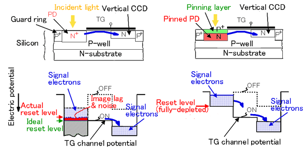
| Fig. 1 Cross section of the pixel of a CCD image sensor that uses a conventional photodiode and illustration showing its electrical potential | Fig. 2 Cross section of the pixel of a CCD image sensor that uses an embedded PD and illustration showing its electrical potential |

|
Fig. 3 Effect of reducing dark current and pixel-to-pixel variation (fixed pattern noise) t of - pinned PD; (a) conventional PD, (b) pinned PD |
With the conventional PD, unevenness in dark current is seen in the portion of the chin where the amount of incident light is small, thereby deteriorating the image quality, whereas with the pinned PD such unevenness is totally suppressed.
Meaning of the achievements
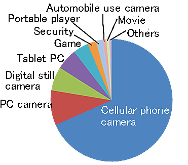
Mass production of the CCD image sensors that used the pinned PD was started in 1987, and it contributed to the widespread use of movies and compact digital cameras. Mass production of the CMOS image sensors that used the pinned PD was started in 2002, and it contributed greatly to the widespread use of cameras for cellular phones. Moreover, application of the sensors was enlarged to various markets such as those for converting standard movies into HDTV movies and of digital single-lens reflex cameras. In 2011 the number of the sensors sold reached 2.1 billion pieces and the pinned PD was used in almost all the sensors. Fig. 4 shows the ratios of the number of pieces sold in 2011 for each of the applications. Those for use for cellular phone cameras account for a large proportion, being 68%, followed by PC cameras, digital still cameras, tablet PCs, games, and security in the order of the number of pieces sold. Although the number of pieces sold is small, image sensors for medical, industrialand scientific applications play important roles. Furthermore, development of distance measuring image sensors for gesture input and as automobile use camera as well as photon counting image sensors for cell observation is anticipated.
|
Fig. 4 Number of area image sensors sold for each of the applications (2011)
(Source: Techno Systems Research Co., Ltd.)
|