The 16th (2016) Yamazaki-Teiichi Prize Winner Semiconductor & Semiconductor Device
Realization of superior characteristic quantum dot lasers with optical communication wavelength and its commercialization with mass-production
| Winner | ||
|---|---|---|
| Mitsuru Sugawara | ||
| History | ||
| Mar. 1982 | Bachelor degree, Department of Applied Physics, The University of Tokyo | |
| Mar. 1984 | Master's Degree, Department of Applied Physics, School of Engineering, The University of Tokyo | |
| Apr. 1984 | Joined Fujitsu Laboratories Ltd. | |
| May 1995 | Doctor of Engineering, The University of Tokyo | |
| Apr. 2005 | Deputy Manager, Nanotechnology Research Center, Fujitsu Laboratories Ltd. | |
| Apr. 2006 | President and CEO of QD Laser, Inc. | |
| Present | ||
| Winner | ||
|---|---|---|
| Keizo Takemasa | ||
| History | ||
| Mar. 1993 | Graduated from Department of Applied Physics, Faculty of Engineering, The University of Tokyo | |
| Mar. 1995 | Graduated from Department of Applied Physics, School of Engineering, The University of Tokyo | |
| Apr. 1995 | Entered Oki Electric Industry Co., Ltd. | |
| Nov. 2008 | Entered QD Laser, Inc. | |
| Jul. 2016 | Executive Officer/General Manager, Laser Device Division, QD Laser, Inc. | |
| Present | ||
| Winner | ||
|---|---|---|
| Kenichi Nishi | ||
| History | ||
| Mar. 1983 | Graduated from Department of Physics, The University of Tokyo | |
| Apr. 1983 | Entered NEC Corporation | |
| Sep. 2002 | Doctor of Philosophy in Engineering, The University of Tokyo | |
| Apr. 2008 | Entered QD Laser, Inc.; Manager, Wafer Process Development Department, Laser Device Division | |
| Apr. 2015 | Deputy General Manager, Laser Device Devision, QD Laser, Inc. | |
| Present | ||
Reason for award
In 1982, Professors Arakawa and Sakaki proposed a quantum dot laser, which confined carriers in a three-dimensional space. In principle, it meant a greater reduction in the temperature dependency of the threshold characteristics compared to the case of the quantum well laser, which enabled only one-dimensional confinement of the carriers. However, the fabrication of uniform and high-density quantum dots was found to be difficult and could not be achieved. Under these circumstances, Dr. Sugawara, at Fujitsu Laboratories Ltd., further developed the technology to grow self-organized quantum dot crystals. In 1998, he succeeded, for the first time in the world, in achieving the continuous oscillation of quantum dot lasers in a communication wavelength band (1.3μm) at room temperature. Moreover, in an academic-industrial alliance with the University of Tokyo, he further advanced research and development to succeed in the experimental production of a quantum dot laser, which had characteristics superseding those of the InP-based quantum well lasers and, in particular, had less temperature dependency.
In 2006, Dr. Sugawara established QD Laser, Inc. as a business venture originating in Japan. In collaboration with Mr. Takemasa and Dr. Nishi, he further achieved the uniformity of quantum dots and the densification in the surfaces, with twice the density as compared to the conventional ones. Furthermore, he used multi-stratification and device structure optimization to develop a quantum dot laser for communication, which showed stable operation at high temperatures. With the development of a highly reliable crystal growth technique, which achieved a yield of 98 percent or higher, and the corresponding technology for the process, he succeeded in achieving sustained mass-production. Consequently, by making use of quantum dots with characteristics superseding those of conventional InP-based quantum-well lasers (a wide working-temperature range, low power consumption, and long lifetime), and with the advantage of a low price resulting from the use of a GaAs substrate, he achieved a shipment volume exceeding three million units for use in the data communication market, by the fiscal year 2015. Further, the verification of application of the quantum dot as a light source for next-generation optical interconnections has begun. Its contribution to the future ICT society is expected to be considerably higher.
Based on the above considerations, it has been determined that the aforementioned persons, viz. Dr. Sugawara, Mr. Takemasa, and Dr. Nishi, should be the prizewinners of the 16th Yamazaki-Teiichi Prize in Semiconductor and Semiconductor Devices.
Background of research and development
In 1982, Professors Arakawa and Sakaki from the University of Tokyo proposed a quantum dot laser that confined carriers in a three-dimensional space (Fig. 1). They established the a reduced temperature dependency of threshold characteristics as compared to that of the quantum well laser, which confined carriers in a one-dimensional direction. To achieve the high performance expected there, it was necessary to form quantum dots having a size of 10 nm, uniformly and with a high density. Initially, this was thought to be a difficult task. However, Sugawara at Fujitsu Laboratories Ltd. advanced the technique for the growth of self-organized InAs quantum dot crystals based on Molecular Beam Epitaxy (MBE) and the development of laser technology. In 1998, he succeeded, for the first time in the world, in achieving the continuous oscillation of the quantum dot laser in a communication wavelength band (1.3μm) at room temperature. Further, in the academic-industrial alliance with the University of Tokyo, he also succeeded in the experimental production of quantum dot lasers with characteristics superseding those of the conventional InP quantum well lasers, which, in particular, had less temperature dependability.
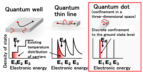
Fig. 1 Discrete density of state of a quantum dot structure Comparisons with a quantum well and thine line
Achievements
In 2006, Sugawara tried to commercialize and mass-produce quantum dot lasers for application in the fields of optical communication and optical interconnection by establishing a business venture―QD Laser, Inc. Along with Takemasa and Nishi, who switched their careers from a major electrical manufacturer in Japan, he further advanced the performance of the quantum dot lasers to a higher level and created a technology for mass-production.
First, they used MBE to control the growth temperature and the volume of material supply continuously, with a time resolution of seconds, and pursued the self-sustained self-forming process of InAs quantum dots. They tried to achieve the optimal conditions for high-density nucleation and the control of the dimensions. As a result, they achieved the multiplication of the density in dot surfaces (6×1010cm-2), multi-stratification (eight strata or more), and a high uniformity (two thirds of the conventional luminescence half width) (Fig. 2).
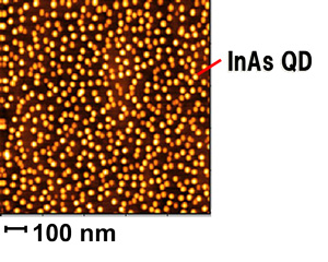
Fig. 2-1 An AFM image of quantum dots (Density:6×1010cm-2)
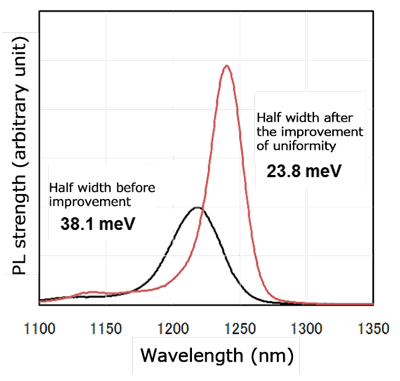
Fig. 2-2 Comparison of the quantum dots in luminescence spectra before and after improvement of uniformity
Simultaneously, they designed a semiconductor laser setup that activated quantum dots and acquired a stable single-mode operation and high reliability. They also advanced the horizontal specialization in the chipping process and the package assembling process in collaboration with national and international manufactures, establishing the technology for the mass-production of quantum dot lasers with a yield of 98 percent or higher.
Fig. 3 shows a mass-produced quantum dot laser characterized by a high operating temperature (100℃ or higher) and the temperature stabilizing operation. By making use of the characteristics superseding those of the conventional InP-based quantum well lasers (a wide working temperature range, low power consumption at a temperature of 50℃ or higher, and long lifetime (300,000 hours at 85℃)) and the advantage of a low price based on the GaAs substrate in use, more than three million units were shipped to the data communication market in the fiscal year 2015. At present, they are advancing the application to high temperature environments for the communications among mobile phone base stations and the like, where the temperature exceeds 100℃.
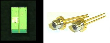
Fig. 3-1 A quantum dot laser chip and TO-CAN package
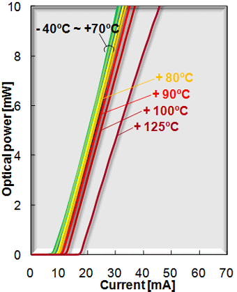
Fig. 3-2 Electric current-optical output characteristics from -40℃ to 120℃
Meaning of the achievements
The three great inventions in the 20th century―the transistor, the laser, and the computer―have reduced in size with an improvement in performance due to the advancements in semiconductor technology, and led to the creation of an internet-based global information platform. In the 21st century, the fusion of the information world with human activity has progressed radically based on the information platform. In order to cope with the volume of data processing, which has been increasing exponentially, acceleration in the production of silicon-based electronic-signal processing systems is needed.
Presently, QD Laser is trying to achieve this, and in cooperation with the Photonics Electronics Technology Research Association (PETRA), is on a fast track to advance the development of a silicon photonics technology that fuses the luminous sources of quantum dot lasers and silicon-based electronic/optical circuits. They have already verified a high-speed transmission independent of temperature (room temperature to 125℃) with a quantum dot laser as a luminous source. This technology is expected to enable the optical connection between chips and the processing performance of servers should be greatly enhanced along with a reduction in power consumption.