SCM : Scanning Capacitance Microscopy
SNDM : Scanning Nonlinear Dielectric Microscopy
Features
SCM/SNDM is a measurement method that visualizes the carrier distribution in two dimensions by scanning the sample surface using a conductive probe. The instruments are additional features of an atomic force microscopy (AFM) system.
- Carrier density range : 1015~1020cm-3(SCM); 1014~1020cm-3(SNDM)
- Identification of semiconductor type (p- or ntype).
- Only relative carrier concentrations can be measured.
- Simultaneous AFM image acquisition possible.
Application Examples
- Identification of diffusion layer carrier polarity.
- Diffusion layer shape at a specific location in LSIs.
- Diffusion layer shape in discrete semiconductor components, e.g., bipolar transistors, diodes, double-diffused metal oxide semiconductor (DMOS), and insulated gate bipolar transistors (IGBT).
- Diffusion layer shape of defective regions in semiconductor devices, e.g., ion implantation defects, leak defects.
- Diffusion layer shape in thin-film transistors (TFTs); visualization of the lightly doped drain (LDD) regions.
- Polarization of ferroelectric materials.
Principle of operation
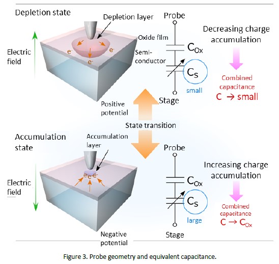
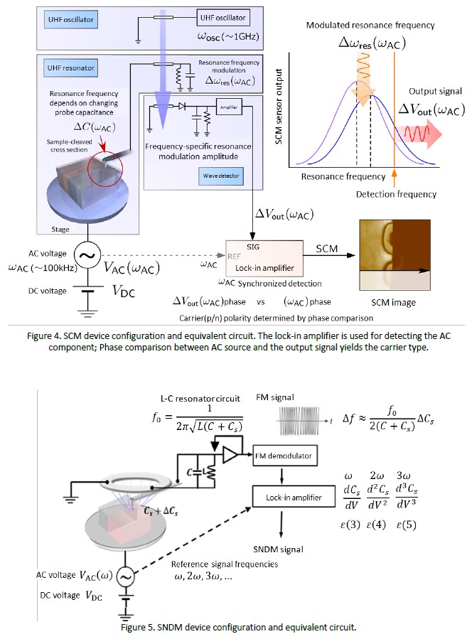
SCM/SNDM basically provides a visualization of the carrier distribution by measuring the change in capacitance between the AFM probe and the sample. The contact point between the probe and the sample constitutes a MOS structure and can electrically be regarded as a system in which the capacitance COx of the oxide film on the semiconductor surface and the capacitance CD of the semiconductor are electrically connected. When a high frequency voltage VAC is applied to this system, the total capacitance 𝐶𝐶 fluctuates. This fluctuation is due to the vibration of carriers in the semiconductor just below the probe, and the magnitude of Figure 1. Photograph of the SCM equipment and its components. Figure 2. Photograph of the SNDM equipment and its components.. Scanning Capacitance Microscopy (SCM) Scanning Nonlinear Dielectric Microscopy (SNDM) Page 2 of 6 the fluctuation depends on the corresponding carrier concentration. The carrier 2D distribution can therefore be imaged by scanning the probe in two orthogonal directions while measuring the modulation signal of the high-frequency resonator caused by the variation Δ𝐶𝐶 of the combined capacitance 𝐶.
Data examples
Planar insulated gate bipolar Si transistor. Fig.6 shows the n- and p-type regions in blue and orange, respectively. The relationship between the carrier concentration and the SCM signal is shown to the right of Fig.6 in the right figure. The carrier densities are not absolute because the shape of the characteristic curve changes depending on the conditions of the needle tip and the sample surface.
Figure 7 (left) shows an AFM image of the cross section exposed by polishing. Since the polishing rate differs depending on the material, the structure such as wiring appears uneven surface. Figure 7 (right) shows a composite AFM/SCM image where the positional relationshipbetween the wiring and the diffusion layer can be identified.
Data format of deliverables
Specifications
Items for enquiries
- Purpose and scope of the analysis
- Sample information:
- Number of samples, availability of preliminary samples.
- Measurement location (CAD drawing or optical micrograph) , cross-sectional shape, diffusion layer shape, type of material, expected carrier polarity and concentration, desired field of view for measurement, etc.
- Handling instructions.
- Preferred due date for preliminary analysis report.
- Due date for delivery of final report.
*Priority order in the case of a large number of samples
- Additional relevant information
Caution
- Samples processed for measurement will not be returned.
- Conversion to absolute value of carrier concentration is not possible.
[SCM]走査型静電容量顕微鏡法・[SNDM]走査型非線形誘電率顕微鏡法の分析事例はこちらからご覧ください。